Array substrate and manufacturing method thereof, display panel and display device

A technology for array substrates and display panels, which is applied in the fields of array substrates and their manufacturing methods, display panels and display devices, can solve problems such as etching process corrosion, low product yield, and short-circuit of data grid lines, etc., to provide products with good quality rate, reducing the probability of DGS, and reducing the effect of corrosion

Inactive Publication Date: 2019-10-18
BOE TECH GRP CO LTD +1
View PDF11 Cites 4 Cited by
  • Summary
  • Abstract
  • Description
  • Claims
  • Application Information

AI Technical Summary

Problems solved by technology

However, the density of the insulating layer 101 is low, which will lead to the peripheral wiring area of ​​the display panel (such as figure 1 The area A and area B) in the area are corroded due to the subsequent etching process, thus appearing similar to the phenomenon of tip discharge, such as figure 2 As shown, data gate short (Data Gate Short, DGS) is prone to occur, resulting in low product yield

Method used


Image

  • Array substrate and manufacturing method thereof, display panel and display device
  • Array substrate and manufacturing method thereof, display panel and display device
  • Array substrate and manufacturing method thereof, display panel and display device

Examples


Embodiment Construction

[0036] In order to make the purpose, technical solutions and advantages of the embodiments of the present disclosure clearer, the technical solutions of the embodiments of the present disclosure will be clearly and completely described below in conjunction with the drawings of the embodiments of the present disclosure. Apparently, the described embodiments are some of the embodiments of the present disclosure, not all of them. Based on the described embodiments of the present disclosure, all other embodiments obtained by persons of ordinary skill in the art without creative effort fall within the protection scope of the present disclosure.

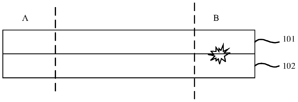
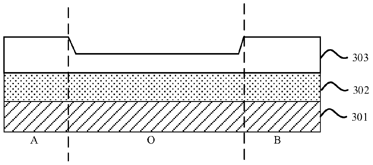
[0037] The inorganic insulating layer on the source-drain metal layer of the current array substrate usually has a double-layer metal layer structure. In order to avoid the oxidation of the source-drain metal layer by the inorganic insulating layer as much as possible, an inorganic insulating film with low density is usually used. However,...


PUM


Abstract

The invention discloses an array substrate and a manufacturing method thereof, a display panel and a display device, which are used for reducing the probability of DGS generation of a display device and improving the yield of an array substrate. The array substrate comprises a substrate, a source-drain electrode metal layer located on the substrate and an inorganic insulating layer located on thesource-drain electrode metal layer. The array substrate comprises a display area and a peripheral area surrounding the display area. The inorganic insulating layer has a first thickness in the displayarea and a second thickness in the peripheral area, wherein the first thickness is smaller than the second thickness.

Description

technical field [0001] The present application relates to the technical field of semiconductors, and in particular to an array substrate and a manufacturing method thereof, a display panel and a display device. Background technique [0002] See figure 1 In an array substrate of a display device, an insulating layer 101 is usually disposed on the source-drain metal layer to protect the source-drain metal layer 102 . Since the source-drain metal layer 102 is usually a double-layer metal layer structure, such as a double-layer copper (Cu) structure, if the insulating layer 101 is silicon oxide (SIO) with a relatively dense structure, the source-drain metal layer will 102 is oxidized. Therefore, the current insulating layer 101 adopts a structure with low density. However, the density of the insulating layer 101 is low, which will lead to the peripheral wiring area of ​​the display panel (such as figure 1 The area A and area B) in the area are corroded due to the subsequent ...

Claims


Application Information

Patent Timeline
Patent Type & Authority Applications(China)
IPC IPC(8): H01L27/12H01L27/32H01L21/84
CPCH01L27/1244H01L27/1248H01L27/1259H10K59/12Y02E10/549Y02P70/50H10K77/10H10K2102/351H10K59/1213
Inventor 王明
Owner BOE TECH GRP CO LTD
Why Eureka
Try Eureka