OLED device structure and fabrication method thereof

A device structure and organic layer technology, applied in the field of microelectronics, can solve problems such as burn-in and short service life of OLED displays, and achieve the effects of reducing intensity, improving light utilization, and strong concentrating effect.

Pending Publication Date: 2019-10-18
FUJIAN HUAJIACAI CO LTD
View PDF0 Cites 0 Cited by
  • Summary
  • Abstract
  • Description
  • Claims
  • Application Information

AI Technical Summary

Problems solved by technology

[0003] However, due to the restriction of the luminous efficiency of organic materials, the service life of OLED displays will not be long, and bad phenomena such as "screen burn-in" will easily occur.

Method used


Image

  • OLED device structure and fabrication method thereof
  • OLED device structure and fabrication method thereof
  • OLED device structure and fabrication method thereof

Examples


preparation example Construction

[0041] A method for preparing an OLED device structure, comprising the following steps:

[0042] S1. A glass layer is provided, and the surface of the glass layer is covered with a first metal layer;

[0043] S2. Forming a first insulating layer and covering the surface of the first metal layer;

[0044] S3, forming a semiconductor layer and covering the surface of the first insulating layer;

[0045] S4, forming a second insulating layer and covering the surface of the semiconductor layer;

[0046] S5, forming a second metal layer and covering the surface of the second insulating layer;

[0047] S6, forming a third insulating layer and covering the surface of the second metal layer;

[0048] S7, forming a first organic layer and covering the surface of the third insulating layer, forming a groove in the first organic layer, the vertical cross-sectional shape of the groove is arc-shaped;

[0049] S8, forming a third metal layer and covering the surface of the first organic...

Embodiment 1

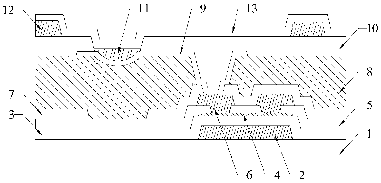
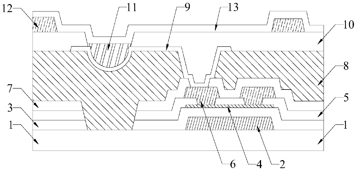
[0069] Please refer to Figure 1 to Figure 3 , Embodiment 1 of the present invention is:

[0070] An OLED device structure, comprising a glass layer 1, on the surface of the glass layer 1, a first metal layer 2, a first insulating layer 3, a semiconductor layer 4, a second insulating layer 5, a second metal layer 6, The third insulating layer 7, the first organic layer 8, the third metal layer 9, the second organic layer 10, the fourth metal layer 12 and the third organic layer 13, the first organic layer 8 is provided with grooves, so The vertical section shape of the groove is arc-shaped, the second organic layer 10 is provided with a first via hole, the first via hole is opposite to the groove, and the first via hole is filled with There is an OLED light-emitting layer 11, one side of the OLED light-emitting layer 11 is in contact with a side of the third metal layer 9 away from the glass layer 1, and the other side opposite to the one side of the OLED light-emitting layer...

Embodiment 2

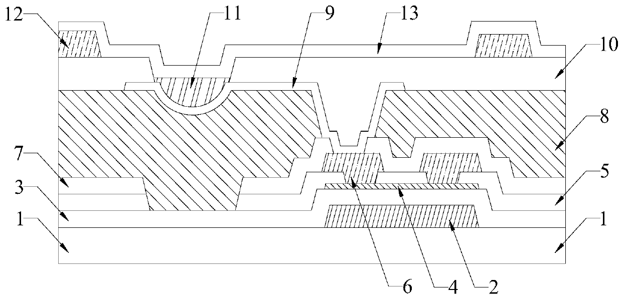
[0079] Please refer to Figure 4 , the second embodiment of the present invention is:

[0080] A method for preparing an OLED device structure, comprising the following steps:

[0081] S1. A glass layer 1 is provided, and the surface of the glass layer 1 is covered with a first metal layer 2;

[0082] S2, forming a first insulating layer 3 and covering the surface of the first metal layer 2;

[0083] S3, forming a semiconductor layer 4 and covering the surface of the first insulating layer 3;

[0084] S4, forming a second insulating layer 5 and covering the surface of the semiconductor layer 4;

[0085] S5, forming a second metal layer 6 and covering the surface of the second insulating layer 5;

[0086] S6, forming a third insulating layer 7 and covering the surface of the second metal layer 6;

[0087] S7, forming a first organic layer 8, and covering the surface of the third insulating layer 7, forming a groove in the first organic layer 8, the vertical cross-sectional...


PUM


Abstract

The invention relates to the technical field of microelectronics, in particular to an OLED device structure and a fabrication method thereof. The OLED device structure comprises a glass layer, a firstmetal layer, a first insulation layer, a semiconductor layer, a second insulation layer, a second metal layer, a third insulation layer, a first organic layer, a third metal layer, a second organic layer, a fourth metal layer and a third organic layer. A groove is formed in the first organic layer, the vertical cross section of the groove is in an arc shape, a microstructure similar to a concavemirror can be formed, the concave mirror is high in condensation effect, the light ray utilization rate of an OLED light-emitting layer can be effectively improved, and the display effect of a panel is improved. In the OLED device structure designed by the scheme, the current intensity can be reduced under the condition that same brightness is achieved, the service lifetime of a light-emitting material is prolonged, and the device brightness is more excellent under the same light-emitting area.

Description

technical field [0001] The invention relates to the technical field of microelectronics, in particular to an OLED device structure and a preparation method thereof. Background technique [0002] Organic Light Emitting Diode (OLED for short) has the advantages of self-illumination, wide viewing angle, high contrast, low power consumption, high response rate, full color and simple manufacturing process, etc., and OLEDs using flexible backplane materials can make Display products are lighter, thinner, bendable and not easy to break, which is the trend of OLED display development in the future. [0003] However, due to the restriction of the luminous efficiency of organic materials, the service life of the OLED display will not be long, and bad phenomena such as "screen burn-in" will easily occur. Therefore, it is particularly necessary to provide an OLED device structure and a preparation method thereof to improve the light utilization efficiency of the OLED device. Contents...

Claims


Application Information

Patent Timeline
Patent Type & Authority Applications(China)
IPC IPC(8): H01L51/52H01L51/56
CPCH10K50/856H10K50/86H10K71/00
Inventor 陈宇怀黄志杰苏智昱
Owner FUJIAN HUAJIACAI CO LTD
Why Eureka
Try Eureka