

Antenna structure
A technology of antenna structure and conductive parts, applied in the direction of antenna, antenna grounding switch structure connection, antenna grounding device, etc., can solve the problem of not being able to cover 4G and 5G frequency bands at the same time, and achieve the effect of suppressing mutual influence
- Summary
- Abstract
- Description
- Claims
- Application Information
AI Technical Summary
Problems solved by technology
Method used
Image

Examples
no. 1 example
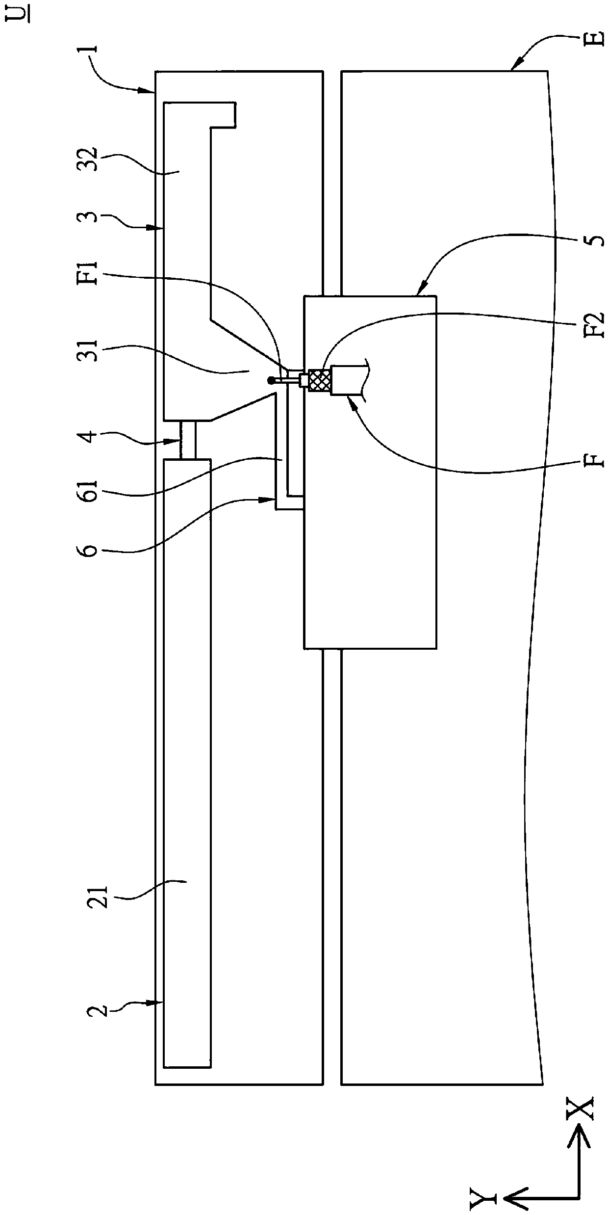
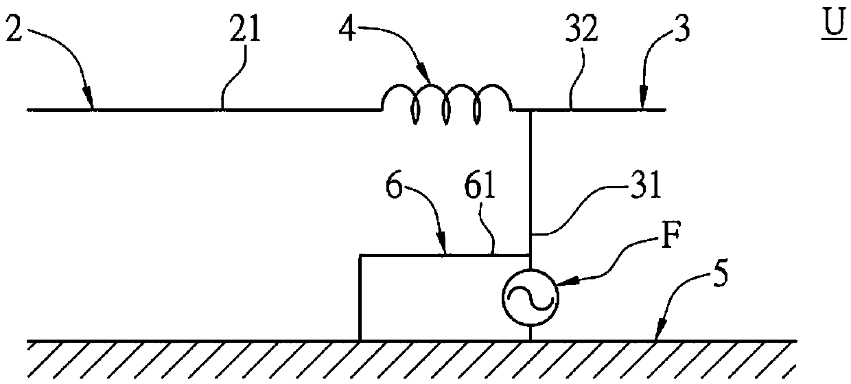
[0047] First, see figure 1 and figure 2 , figure 1 It is one of the schematic top views of the antenna structure of the first embodiment of the present invention, that is, the schematic diagram of the antenna structure implemented on the substrate, figure 2 It is a schematic diagram of the circuit structure of one implementation of the antenna structure of the first embodiment of the present invention. The present invention provides an antenna structure U, which includes a substrate 1, a first radiating element 2, a second radiating element 3, a first inductance 4, a grounding element 5, a first conductive element 6 and a feed-in piece f. The first radiating element 2 , the second radiating element 3 , the first inductor 4 and the first conductive element 6 can be disposed on the substrate 1 , and the first inductor 4 can be coupled between the first radiating element 2 and the second radiating element 3 In other words, one end of the first inductor 4 (not labeled in the...
no. 2 example
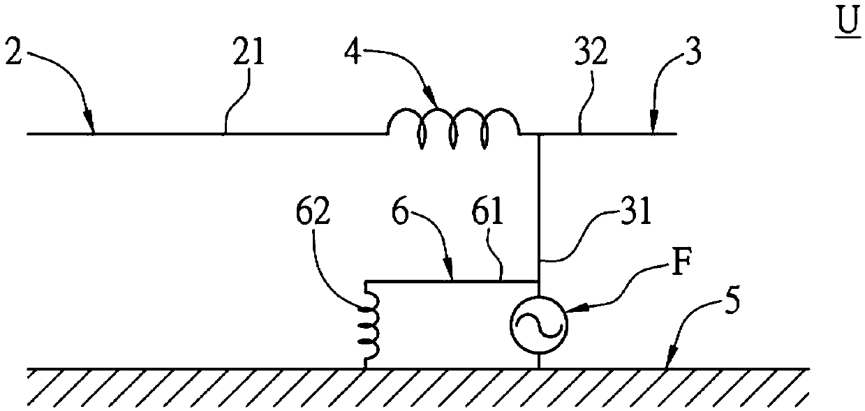
[0055] First, see Figure 4 , Figure 4 It is a schematic circuit diagram of one implementation of the antenna structure of the second embodiment of the present invention. Depend on Figure 4 and figure 2 Comparison shows that the difference between the second embodiment and the first embodiment is that the antenna structure U provided by the second embodiment may further include a stub 7 (stub). Thereby, by setting the residual band 7, the center frequency of the third frequency band range in the second operating frequency band can be adjusted.
[0056] Based on the above, further speaking, the residual strip 7 can be disposed on the substrate 1 and integrally formed with the first conductive element 6 and the second radiating element 3. At the same time, the residual strip 7 can have an open end 71 and a coupling to the connection end 72 of the first conductive member 6 . According to the embodiment of the present invention, the connection end 72 of the stub 7 is defin...
no. 3 example
[0060] First, see Figure 7 , Figure 7 It is a schematic diagram of the circuit structure of one implementation of the antenna structure of the third embodiment of the present invention. Depend on Figure 7 and figure 2 The comparison shows that the difference between the third embodiment and the first embodiment is that: the antenna structure U provided by the third embodiment can further include a parasitic element P, whereby, through the setting of the parasitic element P, the second Gains of the first frequency band range and the second frequency band range in the operating frequency band.
[0061] Based on the above, further speaking, the parasitic element P can be disposed on the substrate 1 and adjacent to the second radiation portion 32 . In addition, one end of the parasitic element P can be coupled to the ground element 5. In the third embodiment, the parasitic element P can have a first parasitic portion P1 coupled to the ground element 5 and a bend from the f...
PUM
 Abstract
Description
Claims
Application Information