Supercharge Your Innovation With Domain-Expert AI Agents!

Chip self-destruction circuit and destruction method based on chip self-destruction circuit

A self-destruction, chip technology, applied in the direction of circuits, electrical components, electric solid devices, etc., can solve the problems of high hardware cost and low destruction efficiency, and achieve the effect of reducing hardware cost, high destruction efficiency and simple structure

Active Publication Date: 2019-10-22
SAGE MICROELECTRONICS CORP
View PDF6 Cites 0 Cited by
  • Summary
  • Abstract
  • Description
  • Claims
  • Application Information

AI Technical Summary

Problems solved by technology

[0004] The embodiment of the present application provides a chip self-destruction circuit and a destruction method based on the chip self-destruction circuit, which are used to solve the problem of low destruction efficiency in the prior art in which an external physical destruction circuit or a dedicated physical destruction device is used to destroy the chip. And the problem of high hardware cost

Method used


Image

  • Chip self-destruction circuit and destruction method based on chip self-destruction circuit
  • Chip self-destruction circuit and destruction method based on chip self-destruction circuit
  • Chip self-destruction circuit and destruction method based on chip self-destruction circuit

Examples


Embodiment 1

[0036] In order to solve the problem of low destruction efficiency and high hardware cost in the prior art in which an external physical destruction circuit or a dedicated physical destruction device is used to destroy a chip, Embodiment 1 of the present application provides a chip self-destruction circuit.

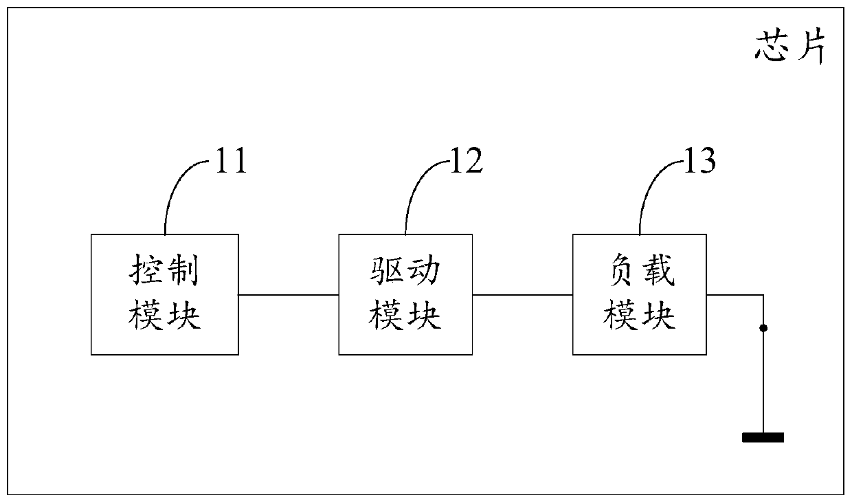
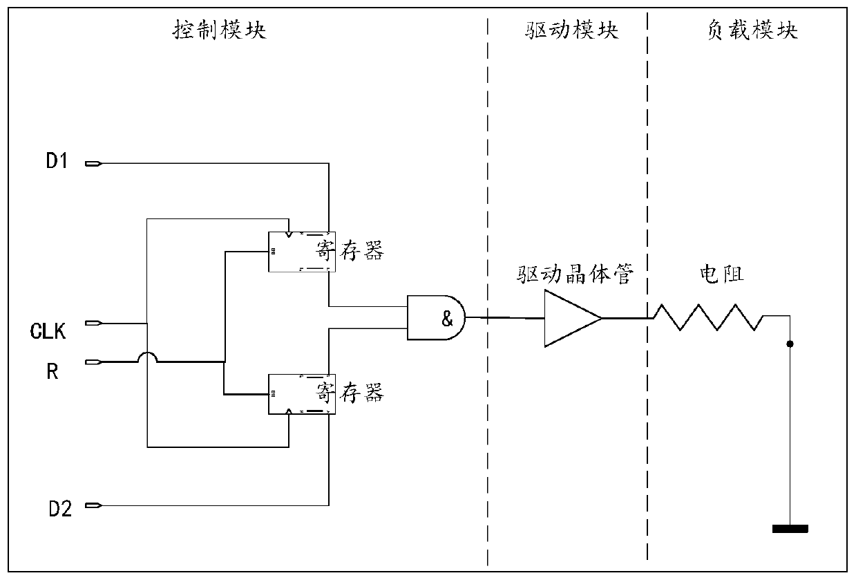
[0037] See the attached figure 1 , figure 1 A schematic structural diagram of a chip self-destruction circuit provided in Embodiment 1 of the present application. The chip self-destruction circuit is applied inside the chip and includes a control module 11, a drive module 12, and a load module 13 connected in sequence. The load module 13 One end is grounded, and the other end is connected to the drive module 12, wherein:

[0038] The control module 11 is used to output a high level, so that the self-destruction circuit of the chip is turned on;

[0039] The drive module 12 is used to burn the chip when the current formed after the chip is turned on from the destruction ...

Embodiment 2

[0058] In order to solve the problem of low destruction efficiency and high hardware cost in the prior art of destroying chips by connecting an external physical destruction circuit or using a special physical destruction device, Embodiment 2 of the present application provides a chip self-destruction circuit-based Destroy method.

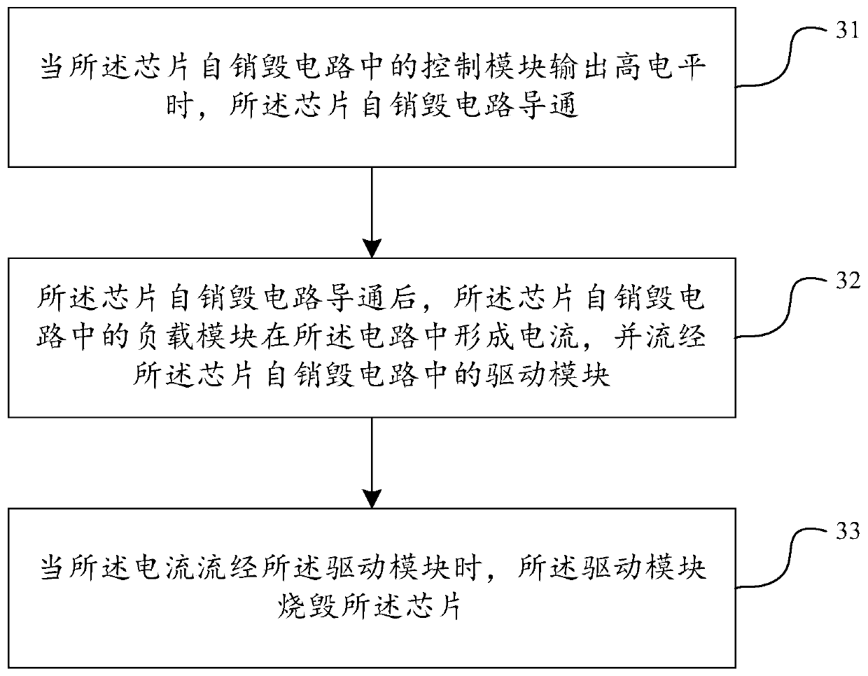
[0059] See attached image 3 , image 3 It is a schematic flow diagram of a destruction method based on a chip self-destruction circuit provided in Embodiment 2 of the present application. The flow specifically includes the following steps:

[0060] Step 31: When the control module in the chip self-destruction circuit outputs a high level, the chip self-destruction circuit is turned on;

[0061] Step 32: After the chip self-destruction circuit is turned on, the load module in the chip self-destruction circuit forms a current in the circuit, and flows through the drive module in the chip self-destruction circuit;

[0062] Step 33: When the curren...


PUM


Abstract

The invention discloses a chip self-destruction circuit which is applied to the interior of a chip and comprises a control module, a driving module and a load module, wherein the control module, the riving module and the load module are connected in sequence; one end of the load module is grounded, and the other end of the load module is connected with the driving module; the control module is used for outputting a high level so that the chip self-destruction circuit is conducted; the load module is used for forming current in the circuit when the chip self-destruction circuit is conducted; and the driving module is used for burning the chip when the current flows through. The invention further discloses a destruction method based on the chip self-destruction circuit. The problems that inthe prior art, the destruction efficiency is low and the hardware cost is high in a way that a physical destruction circuit is externally connected or a special physical destruction device is used fordestroying the chip.

Description

technical field [0001] The present application relates to the field of chip design technology and the field of information security technology, in particular to a chip self-destruction circuit and a destruction method based on the chip self-destruction circuit. Background technique [0002] With the application and popularization of electronic products, chip technology is also developing vigorously. Many important high-tech technical information are stored inside the chip, such as the bank's magnetic card chip, the memory chip of the storage device, etc. These chips have extremely high requirements on information security, and they usually have access rights to perform security verification when they are used. Therefore, when the chip is illegally invaded by a malicious attacker or is required to give up information, it is necessary to activate the destruction device to destroy the chip to ensure information security. [0003] In the prior art, the chip is usually destroye...

Claims


Application Information

Patent Timeline
Patent Type & Authority Applications(China)
IPC IPC(8): H01L23/00
CPCH01L23/573H01L23/576
Inventor 骆建军刘海銮陈华月
Owner SAGE MICROELECTRONICS CORP
Features
  • R&D
  • Intellectual Property
  • Life Sciences
  • Materials
  • Tech Scout
  • Unparalleled Data Quality
  • Higher Quality Content
  • 60% Fewer Hallucinations
Learn More