Chip of light-emitting diode and its manufacturing method

A light-emitting diode and chip technology, applied in semiconductor devices, electrical components, circuits, etc., can solve problems such as the influence of light-emitting diode uniformity, abnormal light emission of electrode fingers, weak current expansion ability, etc., to reduce breakdown holes and reduce light emission Effects of abnormal conditions and improved current spreading efficiency

Active Publication Date: 2021-06-15
HC SEMITEK SUZHOU
View PDF0 Cites 0 Cited by
  • Summary
  • Abstract
  • Description
  • Claims
  • Application Information

AI Technical Summary

Problems solved by technology

[0004] However, due to the small area of ​​the current current blocking layer, especially the weak current spreading ability in the area where the electrode fingers are located, and the current in the area where the electrode fingers are located is still relatively concentrated, it is easy to have breakdown holes in the epitaxial layer and cause the electrode fingers to appear. Abnormal luminescence will eventually affect the luminous uniformity of LEDs

Method used


Image

  • Chip of light-emitting diode and its manufacturing method
  • Chip of light-emitting diode and its manufacturing method
  • Chip of light-emitting diode and its manufacturing method

Examples


Embodiment Construction

[0038] In order to make the object, technical solution and advantages of the present invention clearer, the implementation manner of the present invention will be further described in detail below in conjunction with the accompanying drawings.

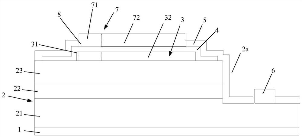
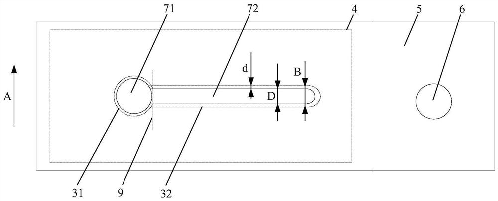
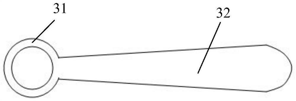
[0039] figure 1 It is a structural schematic diagram of a chip of a light emitting diode provided by an embodiment of the present invention, such as figure 1 As shown, the chip includes a substrate 1 , an epitaxial layer 2 laminated on the substrate 1 , and a current blocking layer 3 , a transparent conductive layer 4 , and a passivation layer 5 sequentially laminated on the epitaxial layer 2 . The chip also includes an n-electrode 6 and a p-electrode 7 , and the epitaxial layer 2 includes an n-type layer 21 , a light-emitting layer 22 , and a p-type layer 23 stacked on the substrate 1 in sequence.

[0040] The epitaxial layer 2 has a groove 2a exposing the n-type layer 21, the n-electrode 6 is placed on the n-type layer 21, the trans...


PUM

PropertyMeasurementUnit
thicknessaaaaaaaaaa

Abstract

The invention discloses a light-emitting diode chip and a preparation method thereof, belonging to the field of light-emitting diode manufacturing. In the light-emitting diode chip of this structure, the current blocking layer is divided into a first part and a second part that are respectively in contact with the pad of the p-electrode and the electrode fingers, and the orthographic projection of the electrode fingers on the surface of the substrate is located at the second In the orthographic projection of the part on the substrate, the area of ​​the orthographic projection of the electrode finger on the surface of the substrate is smaller than the area of ​​the orthographic projection of the second part on the substrate. The second part of the current blocking layer can better realize the expansion of the current in the area where the electrode fingers are located, and can also weaken the situation where the current is too concentrated in the area where the electrode fingers are located and breakdown holes appear in the epitaxial layer, reducing the occurrence of holes in the epitaxial layer. Luminescence abnormality occurs. The current expansion efficiency in the chip of the light-emitting diode is improved, the abnormal light emission is reduced, and the overall light emission uniformity of the chip is improved.

Description

technical field [0001] The invention relates to the field of light-emitting diode manufacturing, in particular to a light-emitting diode chip and a preparation method thereof. Background technique [0002] LED is a light-emitting diode, which is a semiconductor solid-state light-emitting device. LED has the characteristics of energy saving, environmental protection, long life, firm structure, fast response time, etc., and can be widely used in various general lighting, backlighting, display, indication and urban night scenes and other fields. [0003] The current light-emitting diode chip usually includes a substrate, an epitaxial layer grown on the substrate, and a current blocking layer grown sequentially on the epitaxial layer, a transparent conductive layer, and a passivation layer. The chip also includes an n-electrode and a p-electrode. The epitaxial layer usually includes an n-type layer, a light-emitting layer, and a p-type layer grown sequentially on the substrate....

Claims


Application Information

Patent Timeline
Patent Type & Authority Patents(China)
IPC IPC(8): H01L33/14H01L33/38H01L33/00
CPCH01L33/007H01L33/145H01L33/38
Inventor 张春莲李俊生胡根水孙虎
Owner HC SEMITEK SUZHOU
Why Eureka
Try Eureka