Electrode preparation method for improving current expansion and luminous efficiency of GaAs-based light-emitting diode

A light-emitting diode and current expansion technology, which is applied in the field of optoelectronics, can solve the problems of low light extraction efficiency and poor current expansion effect, and achieve the effects of improving current expansion efficiency, improving light extraction efficiency, and avoiding absorption

Inactive Publication Date: 2016-03-30
SHANDONG INSPUR HUAGUANG OPTOELECTRONICS
View PDF7 Cites 8 Cited by
  • Summary
  • Abstract
  • Description
  • Claims
  • Application Information

AI Technical Summary

Problems solved by technology

The present invention aims at the problems of poor current expansion effect of GaAs-based LED chips and low light extraction efficiency caused by electrodes blocking light output, so as to improve the current expansion and light extraction efficiency of GaAs-based LED chips

Method used


Image

  • Electrode preparation method for improving current expansion and luminous efficiency of GaAs-based light-emitting diode
  • Electrode preparation method for improving current expansion and luminous efficiency of GaAs-based light-emitting diode
  • Electrode preparation method for improving current expansion and luminous efficiency of GaAs-based light-emitting diode

Examples


Embodiment 1

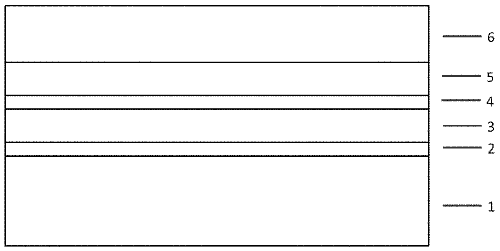
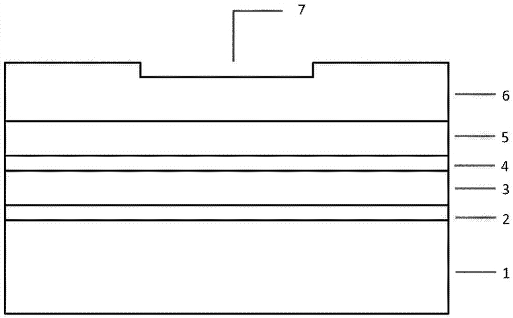
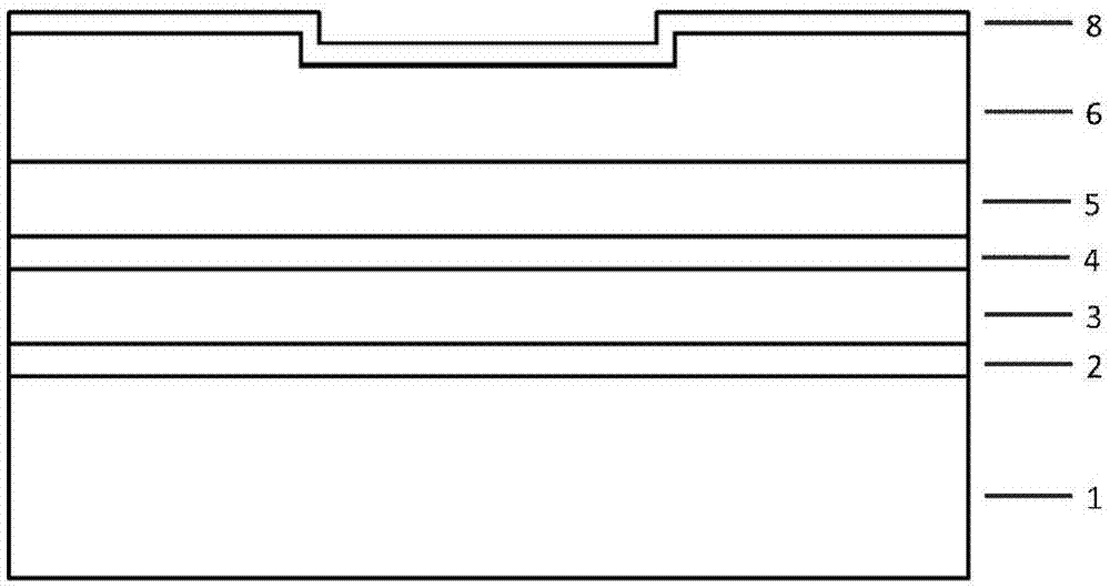
[0038] An electrode preparation method for improving the current expansion and light extraction efficiency of GaAs-based light-emitting diodes, comprising the following steps:

[0039](1) Current blocking area: Utilize photoresist coating and plasma etching to prepare pattern recessed area on GaAs base epitaxial wafer, and remove photoresist; Described step (1) utilizes photoresist coating to refer to GaAs base epitaxial wafer Coat photoresist on the epitaxial wafer, and photolithographically pattern; use a glue spinner to evenly coat a layer of photoresist on the GaAs-based epitaxial wafer, the photoresist is positive photoresist, and the thickness of the photoresist is 1.2-1.5 μm; Use an exposure machine to expose, then develop and harden the film to produce the required photolithographic pattern; use plasma etching to etch the p-type current spreading layer 6 in the photolithographic pattern area to form a current blocking region 7, such as figure 2 As shown, the etching d...

Embodiment 2

[0046] As described in Example 1, the electrode preparation method for improving the current expansion and light extraction efficiency of GaAs-based light-emitting diodes, the difference is that in the step (2), the ITO film is deposited on the GaAs-based epitaxial wafer by magnetron sputtering method completed.

[0047] The method for evaporating a metal thin film on the surface of the GaAs substrate in the step (6) is an electron beam evaporation method.

Embodiment 3

[0049] A kind of electrode preparation method that improves GaAs-based light-emitting diode current expansion and light extraction efficiency as described in embodiment 1, and its difference is that, the lithography pattern described in described step (1) and step (3) is circular; The diameter of the photolithographic pattern in the step (1) is 10±5 μm longer than the diameter of the photolithographic pattern in the step (3).


PUM

PropertyMeasurementUnit
thicknessaaaaaaaaaa
thicknessaaaaaaaaaa
thicknessaaaaaaaaaa

Abstract

The invention discloses an electrode preparation method for improving the current expansion and luminous efficiency of a GaAs-based light-emitting diode, and the method comprises the steps: preparing a patterned recessed region on a GaAs-based epitaxial wafer through photoresist coating and plasma etching, and removing photoresist; depositing an ITO film on the GaAs-based epitaxial wafer, and carrying out the thermal annealing of the ITO film; carrying out sequential vapor plating of a plurality of metal film layers on the ITO film through photoresist coating and electron-beam evaporation, and forming a pattern electrode, wherein the pattern electrode comprises a pasting layer, a reflection layer, a blocking layer, and a welding layer; removing the metal films in a region outside the pattern electrode through employing a peeling method, and completing the preparation of a P electrode of the GaAs-based light-emitting diode; removing the residual photoresist; thinning a GaAs-based substrate of the GaAs-based epitaxial wafer, carrying out the vapor plating of one metal film layer on the surface of the GaAs-based substrate, and completing the preparation of the N electrode of the GaAs-based light-emitting diode. The method improves the current expansion of the GaAs-based light-emitting diode through employing the ITO film.

Description

technical field [0001] The invention relates to an electrode preparation method for improving the current expansion and light extraction efficiency of a GaAs-based light-emitting diode, and belongs to the field of optoelectronic technology. Background technique [0002] Light Emitting Diode (LED) is an optoelectronic device that converts electrical energy into light energy with semiconductor materials, and is the first commercial compound semiconductor to enter the market. It has the characteristics of small size, long life, high photoelectric conversion efficiency, energy saving and environmental protection, etc., and can meet the requirements of various application equipment for thinness and miniaturization, and is widely used in urban lighting, large-screen display, LCD backlight, communication, traffic signs , Lighting etc. [0003] GaAs-based LED refers to a kind of LED that uses GaAs substrate as the substrate, epitaxially grows III-V compound semiconductor materials,...

Claims


Application Information

Patent Timeline
Patent Type & Authority Applications(China)
IPC IPC(8): H01L33/36H01L33/40H01L33/00
CPCH01L33/36H01L33/005H01L33/405
Inventor 汤福国陈康申加兵李晓明徐现刚夏伟
Owner SHANDONG INSPUR HUAGUANG OPTOELECTRONICS
Why Eureka
Try Eureka