Nitride semiconductor light-emitting device

a light-emitting device and semiconductor technology, applied in the direction of semiconductor devices, basic electric elements, electrical appliances, etc., can solve the problems of degrading the uniformity of light emission, insufficient current diffusion function, and current constriction, so as to improve the current diffusion efficiency, reduce the operation voltage, and improve the effect of light emission uniformity

Inactive Publication Date: 2012-04-26
SHARP KK
View PDF4 Cites 27 Cited by
  • Summary
  • Abstract
  • Description
  • Claims
  • Application Information

AI Technical Summary

Benefits of technology

[0015]In view of the above-described problems in the prior-art, an object of the present invention is to improve the current diffusion efficiency in the nitride semiconductor light-emitting device and decrease the operation voltage while obtaining good light emission uniformity and a high optical output even at a high operation current density.

Problems solved by technology

However, if it is attempted to directly apply any of the techniques disclosed in the five above-mentioned Japanese patent documents to the nitride semiconductor light-emitting device, the following problems will be caused.
Further, the increased sheet resistance of the current diffusion layer hinders the sufficient current diffusion function and degrades the uniformity of light emission.
Particularly when high current is applied to the light-emitting device, current constriction occurs and then excess heat is generated at the current constriction portion.
As a result, there is caused a problem that the proportion of non-emissive recombinations of carriers is increased leading to decrease of the optical output.
However, if the areas of the branch electrodes are increased, there is caused a problem that the proportion of absorption of light emitted from the light-emitting layer is increased due to shielding by the branch electrodes, leading to decrease of the optical output of the light-emitting device.

Method used


Image

  • Nitride semiconductor light-emitting device
  • Nitride semiconductor light-emitting device
  • Nitride semiconductor light-emitting device

Examples


embodiment 1

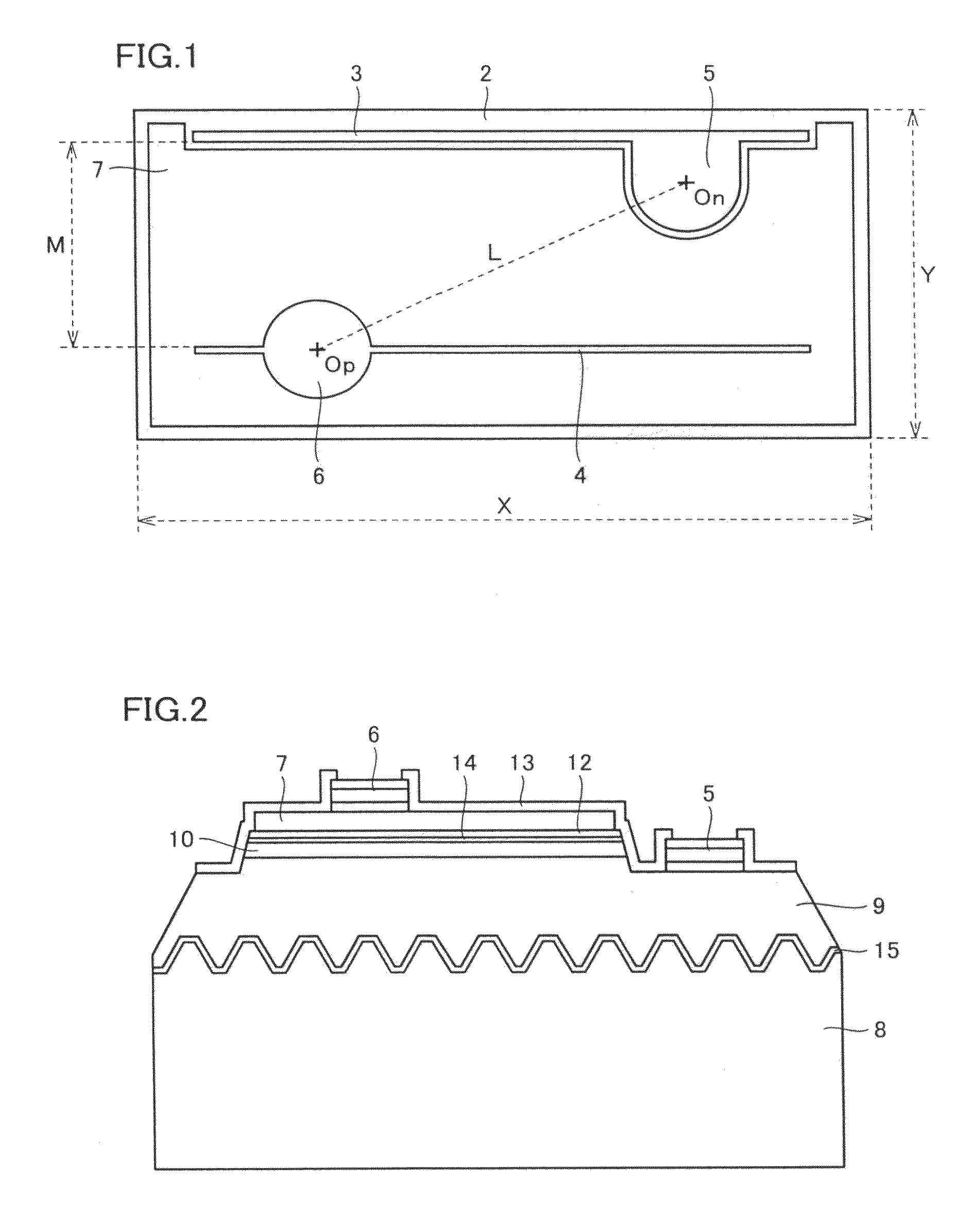
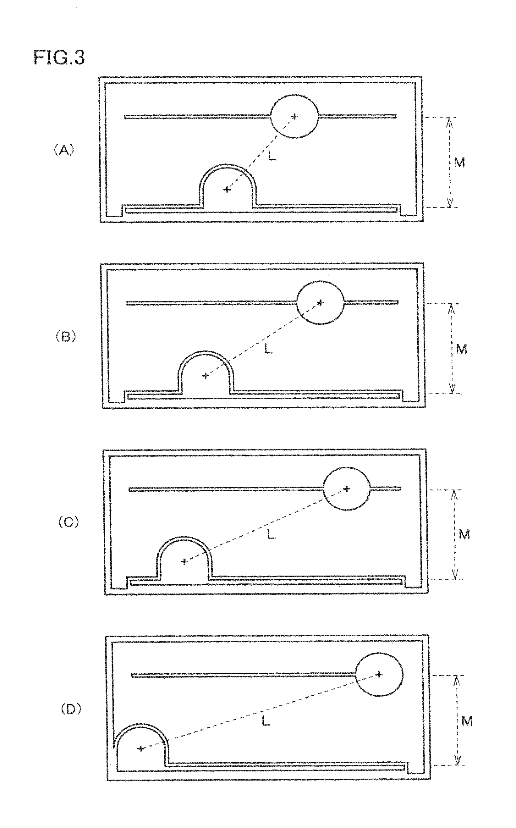
[0046]A light-emitting device similar to that schematically illustrated in FIGS. 1 and 2 is produced in Embodiment 1 of the present invention. FIG. 3(A) shows a schematic plan view of the light-emitting device according to this Embodiment 1.

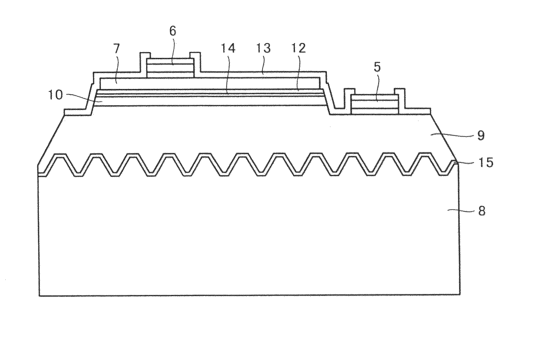
[0047]In the light-emitting device of Embodiment 1, as schematically shown in FIG. 2, an n-type nitride semiconductor layer 9 was deposited on a sapphire substrate 8 having a main surface of a (0001) plane orientation with an intervening AlN buffer layer 15 therebetween. This n-type semiconductor layer 9 includes a GaN underlayer of 9 μm thickness and Si-doped n-type GaN contact layer of 2 μm thickness (carrier concentration: about 6×1018 cm−3) deposited at a substrate temperature of about 1000° C.

[0048]A nitride semiconductor active layer 10 was deposited on n-type semiconductor layer 9. This active layer 10 has a multi-quantum-well structure in which an n-type In0.15Ga0.85N quantum-well layer of 3.5 nm thickness and an Si-doped GaN barrier laye...

embodiment 2

[0057]A light-emitting device according to Embodiment 2 of the present invention is schematically shown in a plan view of FIG. 3(B). The light-emitting device of this Embodiment 2 is different from Embodiment 1 only in that the ratio of M / L was reduced to 0.7, where M represents the distance between the branch electrodes and L represents the distance between the centers of the p-side and n-side electrodes pads. The change of the M / L value in the case of Embodiments 1 and 2 can clearly be seen in comparison between FIG. 3(A) and FIG. 3(B). As clearly seen in FIGS. 6(B) and 6(C), optical output Po (mW) and power efficiency WPE (%) of the light-emitting device of Embodiment 2 (M / L=0.7) are highest in the case that the light-emitting device is operated with current of 100 mA (current density>90 A / cm2; current injection area: 1.10×10⁻³cm2).

embodiment 3

[0058]A light-emitting device according to Embodiment 3 of the present invention is schematically shown in a plan view of FIG. 3(C). The light-emitting device of this Embodiment 3 is different from the other Embodiments only in that the ratio of M / L was further reduced to 0.5, where M represents the distance between the branch electrodes and L represents the distance between the centers of the p-side and n-side electrodes pads.

[0059]FIG. 7 shows photographs of light emission states of the light-emitting devices taken by a CCD camera (HAMAMATU C8000-20). Although the photographs attached hereto are shown as grayscale images, the original photographs are color images in which red, orange, yellow, green, powder blue, blue, and navy blue having different light wavelengths sequentially appear depending on an area emitting high intensity light to an area emitting low intensity light. When such a color photograph is converted to a black-and-white photograph, an area of green having an inte...


PUM


Abstract

A nitride semiconductor light-emitting device includes at least one n-type semiconductor layer, an active layer and at least one p-type semiconductor layer within a rectangle nitride semiconductor region on a substrate. The n-type semiconductor layer has a partial exposed area, a p-side branch electrode integral with a p-side electrode pad formed on a current diffusion layer formed on the p-type semiconductor layer, an n-side branch electrode integral with an n-side electrode pad formed on the partial exposed area of the n-type semiconductor layer, the p-side and n-side branch electrodes extend parallel to each other along two opposite sides of the semiconductor region, and conditions of 0.3<M/L<1.1 and L<Lmax are satisfied; L is the distance between centers of the p-side and n-side electrode pads, M is the distance between the p-side and n-side branch electrodes, and Lmax represents a distance between the centers of the p-side and n-side electrode pads.

Description

[0001]This nonprovisional application is based on Japanese Patent Application No. 2010-235496 filed on Oct. 20, 2010 with the Japan Patent Office, the entire contents of which are hereby incorporated by reference.BACKGROUND OF THE INVENTION[0002]1. Field of the Invention[0003]The present invention is related to a light-emitting device produced utilizing nitride semiconductor (InxAlyGa1-x-yN, 0≦x<1, 0≦y<1) and particularly to a nitride semiconductor light-emitting device usable as a high-luminance light source for a backlight of a liquid crystal display device, usual illumination and so forth.[0004]2. Description of the Background Art[0005]In general, a nitride semiconductor light-emitting device includes an n-type nitride semiconductor layer, a nitride semiconductor light-emitting layer and a p-type nitride semiconductor layer successively stacked on a sapphire substrate. The p-type semiconductor layer side and n-type semiconductor layer side are provided with a p-side electro...

Claims


Application Information

Patent Timeline
Patent Type & Authority Applications(United States)
IPC IPC(8): H01L33/62
CPCH01L33/20H01L33/42H01L33/38
Inventor WENG, YUFENGBROCKLEY, MICHAEL
Owner SHARP KK
Why Eureka
Try Eureka