Light emitting element including metal bulk

a technology metal bulks, applied in the direction of basic electric elements, semiconductor devices, electrical equipment, etc., can solve the problems of deterioration of light emission efficiency, less heat generation of chip scale packages, and poor luminous efficacy of light emitting elements, so as to achieve sufficient light emission regions, improve current spreading efficiency, and good luminous efficacy

Active Publication Date: 2019-05-16
SEOUL VIOSYS CO LTD
View PDF0 Cites 0 Cited by
  • Summary
  • Abstract
  • Description
  • Claims
  • Application Information

AI Technical Summary

Benefits of technology

[0009]Exemplary embodiments of the present disclosure provide a light emitting element that has improved current spreading efficiency and secures a sufficient light emission region to provide good luminous efficacy. In addition, exemplary embodiments of the present disclosure provide a light emitting element which secures reliability through efficient heat dissipation. Furthermore, exemplary embodiments of the present disclosure provide a light emitting element which can be prevented from being damaged due to stress and strain upon separation of a substrate therefrom.
[0010]In accordance with one aspect of the present disclosure, a light emitting element includes: a light emitting structure including a first conductivity type semiconductor layer including a contact region formed on a lower surface thereof, and a mesa including an active layer disposed on the lower surface of the first conductivity type semiconductor layer and a second conductivity type semiconductor layer disposed on a lower surface of the active layer; a second electrode disposed on a lower surface of the second conductivity type semiconductor layer and electrically connected to the second conductivity type semiconductor layer; a first insulation layer disposed on a lower surface and a side surface of the second electrode and including an opening exposing the contact region; an electrode cover layer disposed on a lower surface of the first insulation layer and adjoining the lower surface of the second electrode while being separated from the first electrode; a first electrode disposed on the lower surface of the first insulation layer and adjoining the contact region through the opening; a second insulation layer disposed on the lower surfaces of the first electrode and the electrode cover layer and including openings exposing the first electrode and the second electrode, respectively; and a support structure including a first metal bulk and a second metal bulk disposed on the lower surface and the side surface of the second insulation layer to be separated from each other and electrically connected to the first electrode and the second electrode through the openings, respectively, and an insulating portion disposed on a side surface of the first metal bulk and a side surface of the second metal bulk. The mesa may include a main body and a plurality of protrusions protruding from the main body, and the contact region may be disposed between the protrusions and partially overlap the second metal bulk in a upward-downward direction. With this structure, the light emitting element can prevent the contact region between the first electrode and the first conductivity type semiconductor layer from being excessively biased to one side thereof, thereby improving current spreading efficiency. Therefore, the light emitting element can have further improved luminous efficacy.
[0011]In accordance with another aspect of the present disclosure, a light emitting element includes: a light emitting structure including a first conductivity type semiconductor layer, a second conductivity type semiconductor layer disposed on a lower surface of the first conductivity type semiconductor layer, an active layer interposed between the first conductivity type semiconductor layer and the second conductivity type semiconductor layer, and a plurality of holes formed through the second conductivity type semiconductor layer and the active layer to expose the first conductivity type semiconductor layer; a first electrode disposed in each of the holes and electrically connected to the first conductivity type semiconductor layer; a second electrode insulated from the first electrode, the second electrode being disposed on a lower surface of the second conductivity type semiconductor layer and electrically connected to the second conductivity type semiconductor layer; an insulation layer disposed on a lower surface and a side surface of the first electrode and on a lower surface and a side surface of the second electrode, and having openings exposing the first electrode and the second electrode, respectively; and a support structure including a first metal bulk and a second metal bulk disposed on a lower surface and a side surface of the insulation layer to be separated from each other and electrically connected to the first electrode and the second electrode through the openings, respectively, and an insulating portion disposed on a side surface of the first metal bulk and a side surface of the second metal bulk. In addition, the holes may include a first hole. The first hole includes a first region, a second region, and a connection portion connecting the first region to the second region, in which the first region may be disposed on the first metal bulk and the second region may be disposed on the second metal bulk. With this structure, the light emitting element can have improved current spreading efficiency and can secure a sufficient light emitting region, thereby improving luminous efficacy.
[0012]According to exemplary embodiments, the light emitting element has a contact region extending in a longitudinal direction, thereby preventing the contact region between the first electrode and the first conductivity type semiconductor layer from being biased to one side thereof. As a result, the light emitting element has improved current spreading efficiency. In addition, a light emitting region of the light emitting element can be sufficiently secured by a single mesa structure surrounding the contact region. As a result, the light emitting element can have improved luminous efficacy. Furthermore, the light emitting element can secure efficient heat dissipation through a first metal bulk, a second metal bulk and an electrode cover layer. Furthermore, since the electrode cover layer is formed in a wide region, it is possible to prevent damage to the light emitting element due to stress and strain upon separation of a substrate from the light emitting element.
[0013]Furthermore, according to exemplary embodiments, since the first hole is present over the first metal bulk and the second metal bulk, electric current supplied through the first electrode can be efficiently spread in the light emitting element. Furthermore, the light emitting element can have a sufficient light emitting region, thereby improving luminous efficacy.

Problems solved by technology

A chip scale package structure is more vulnerable to heat generated during high current driving.
If a contact region between the semiconductor layer and the electrode is not sufficient and is present only in a certain region of the light emitting element, the light emitting element allows strong light emission at a certain location of the semiconductor layer due to insufficient spreading of electric current applied from an external power source.
Specifically, since electric current flows to the semiconductor layer only through a certain contact region between the semiconductor layer and the electrode when supplied through the metal bulk, light emission is not efficiently performed in other regions of the semiconductor layer at which the electrode does not contact the semiconductor layer.
Therefore, the light emitting element suffers from deterioration in luminous efficacy.

Method used


Image

  • Light emitting element including metal bulk
  • Light emitting element including metal bulk
  • Light emitting element including metal bulk

Examples


Embodiment Construction

[0045]Light emitting elements according to exemplary embodiments may be realized in various ways.

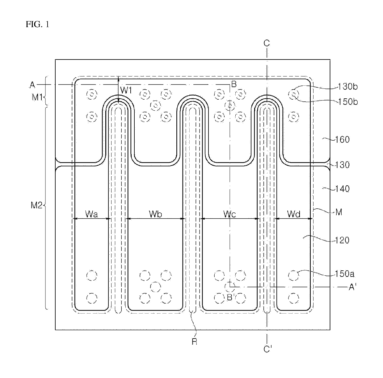
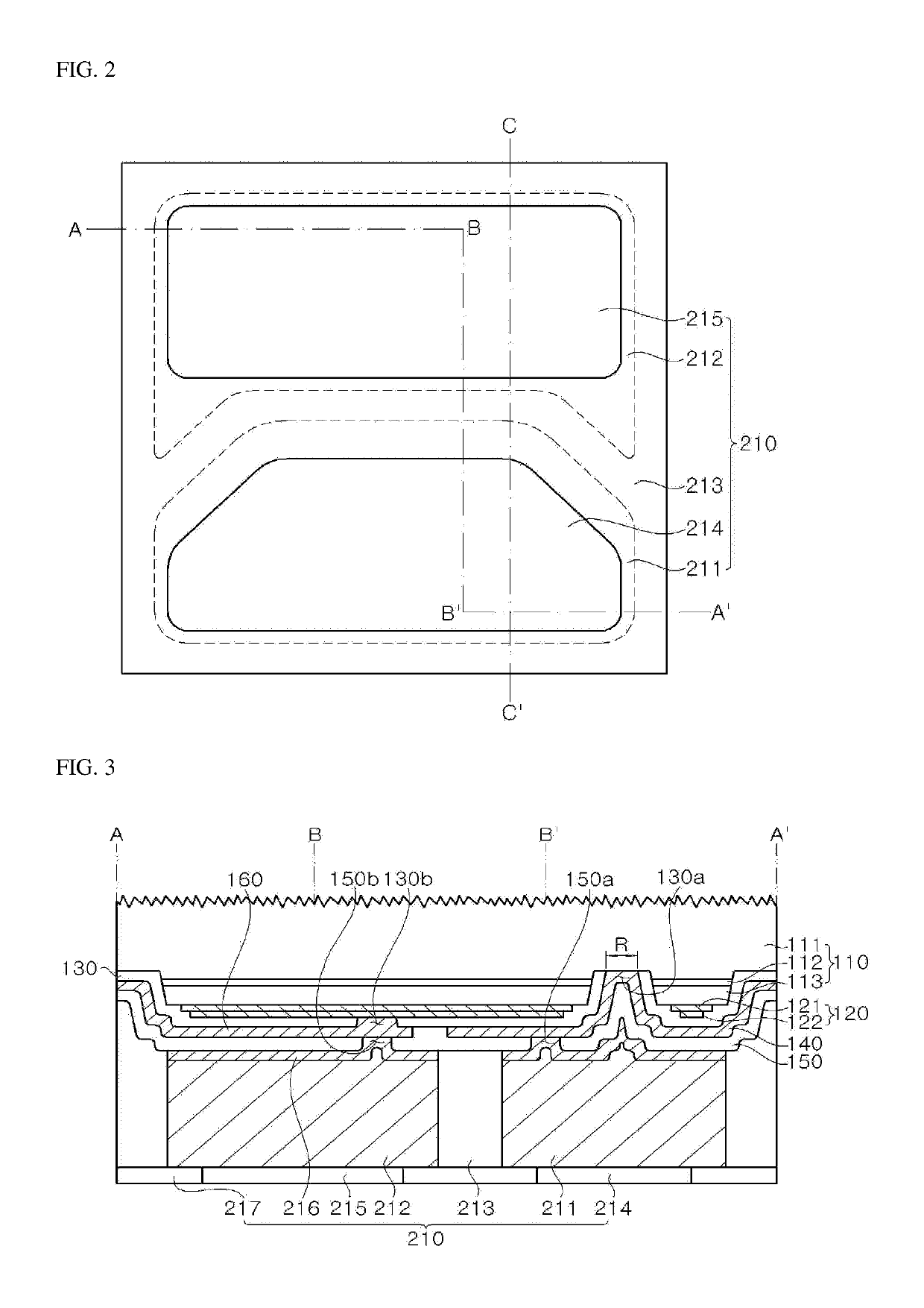
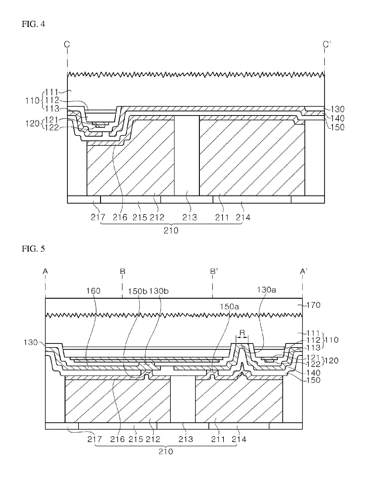
[0046]A light emitting element according to exemplary embodiments includes: a light emitting structure including a first conductivity type semiconductor layer including a contact region formed on a lower surface thereof, and a mesa including an active layer disposed on the lower surface of the first conductivity type semiconductor layer and a second conductivity type semiconductor layer disposed on a lower surface of the active layer; a second electrode disposed on a lower surface of the second conductivity type semiconductor layer and electrically connected to the second conductivity type semiconductor layer; a first insulation layer disposed on a lower surface and a side surface of the second electrode and including an opening exposing the contact region; an electrode cover layer disposed on a lower surface of the first insulation layer and adjoining the lower surface of the second ele...


PUM


Abstract

A light emitting element according to an embodiment of the present invention comprises a first conductive-type semiconductor layer including a contact region on the lower surface thereof, a light emitting structure which includes a mesa including a second conductive-type semiconductor layer and an active layer, a second electrode, a first insulation layer, an electrode cover layer, a first electrode, a second insulation layer, and a support structure. In addition, the mesa may include a body part and a plurality of protrusion parts protruding from the body part, the contact region may be disposed between the protrusion parts, and a part of the contact region may overlap with a second metal bulk in the vertical direction. Accordingly, current spreading efficiency can be improved, and thus luminance efficiency can be more improved.

Description

PRIORITY CLAIMS AND CROSS-REFERENCE TO RELATED APPLICATION[0001]This application is a continuation of U.S. patent application Ser. No. 15 / 558,143, filed on Sep. 13, 2017, which is a National Stage entry under 35 U.S.C. 371 of International Patent Application No. PCT / KR2016 / 002296 filed on Mar. 8, 2016, which claims priority to and the benefit of Korean Patent Application No. 10-2015-0036126, filed on Mar. 16, 2015, and Korean Patent Application No. 10-2015-0037667, filed on Mar. 18, 2015, which are incorporated herein by reference in their entireties for all purposes as if fully set forth herein.TECHNICAL FIELD[0002]Exemplary embodiments of the present disclosure relate to a light emitting element, and more particularly, to a light emitting element having improved luminous efficacy.BACKGROUND[0003]Recently, with increasing demand for small, high power light emitting elements, there is increasing need for a large flip chip type light emitting element having good heat dissipation effi...

Claims


Application Information

Patent Timeline
Patent Type & Authority Applications(United States)
IPC IPC(8): H01L33/38H01L27/15
CPCH01L33/382H01L33/387H01L27/15H01L33/20H01L33/62H01L33/405H01L33/36H01L33/38H01L33/44H01L2933/0016H01L2933/0025
Inventor CHAE, JONG HYEONKIM, CHANG YEONLEE, JOON SUPSUH, DAE WOONGROH, WON YOUNGPARK, JU YONGKIM, SEUNG HYUN
Owner SEOUL VIOSYS CO LTD
Why Eureka
Try Eureka