Method for manufacturing hafnium oxide film
A manufacturing method and technology of hafnium oxide, applied in semiconductor/solid-state device manufacturing, electrical components, semiconductor devices, etc., can solve problems such as uneven structure and uneven thickness of hafnium oxide thin film 103, and achieve the effect of improving uniformity
- Summary
- Abstract
- Description
- Claims
- Application Information
AI Technical Summary
Problems solved by technology
Method used
Image

Examples
Embodiment Construction
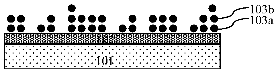
[0040] like Figure 3A to Figure 3E Shown is a device structure diagram in each step of the manufacturing method of the hafnium oxide thin film according to the embodiment of the present invention. The manufacturing method of the hafnium oxide thin film according to the embodiment of the present invention includes the following steps:
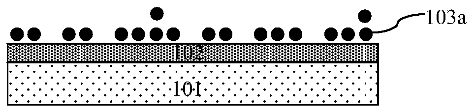
[0041] Step 1, such as Figure 3A As shown, a semiconductor substrate 1 is provided, and the first surface treatment is carried out on the semiconductor substrate 1. The first surface treatment is a displacement treatment, and the first surface treatment is carried out on the semiconductor substrate 1. Formation of hydroxyl distribution.
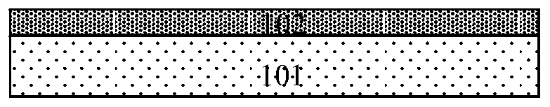
[0042] The semiconductor substrate 1 is a silicon substrate. An interface layer 2 is also formed on the surface of the semiconductor substrate 1 .
[0043] Preferably, the material of the interface layer 2 is silicon oxide.
[0044] The first surface treatment is cleaned with No. 1 solution.
[0045] Ste...
PUM
 Abstract
Description
Claims
Application Information
 - R&D
- Intellectual Property
- Life Sciences
- Materials
- Tech Scout
- Unparalleled Data Quality
- Higher Quality Content
- 60% Fewer Hallucinations
Browse by: Latest US Patents, China's latest patents, Technical Efficacy Thesaurus, Application Domain, Technology Topic, Popular Technical Reports.
© 2025 PatSnap. All rights reserved.Legal|Privacy policy|Modern Slavery Act Transparency Statement|Sitemap|About US| Contact US: help@patsnap.com