

Broadband terahertz wave detector
A detector and terahertz technology, applied in the field of terahertz wave detection, can solve problems such as narrow detection bandwidth, achieve the effect of reducing area and solving narrow detection bandwidth
- Summary
- Abstract
- Description
- Claims
- Application Information
AI Technical Summary
Problems solved by technology
Method used
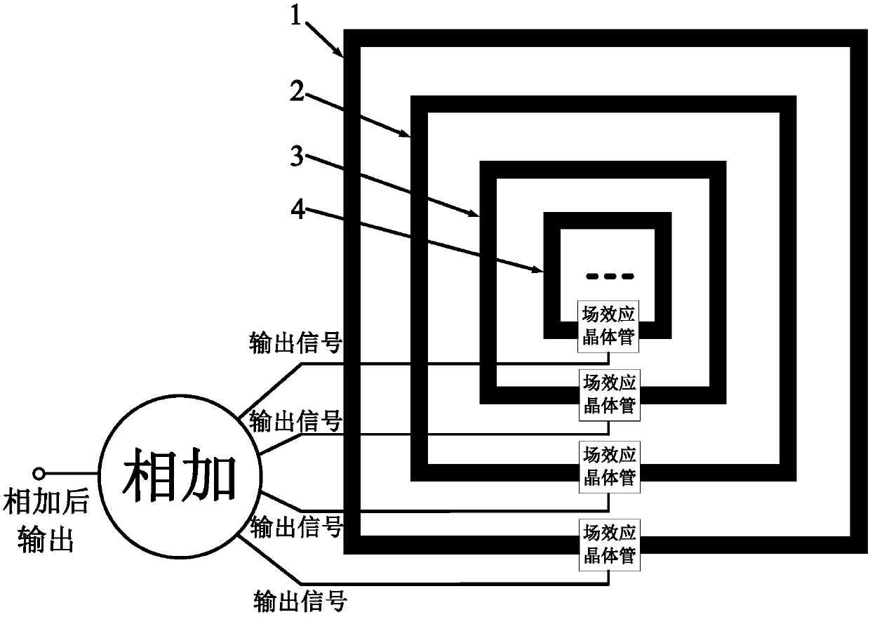
Image

Examples
Embodiment 1
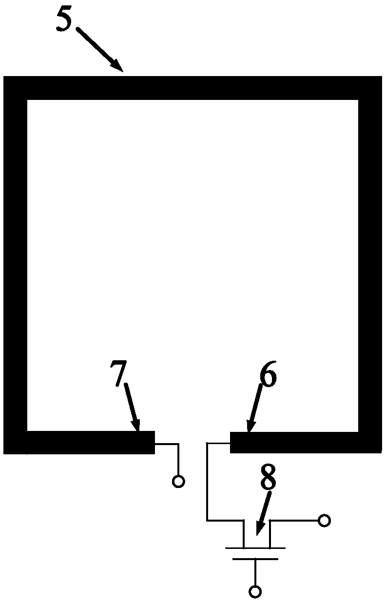
[0035] like figure 2 Shown is a schematic diagram of Embodiment 1 of the connection between the antenna and the field effect transistor of the present invention.
[0036] The first port 6 drawn from the antenna 5 is connected to the source of the field effect transistor 8; the second port 7 drawn from the antenna is grounded or connected to a fixed bias voltage to provide a DC path for the field effect transistor 8, and the field effect transistor A fixed DC bias voltage is applied to the gate of FET 8, and the drain of field effect transistor 8 is used for outputting signals.
Embodiment 2
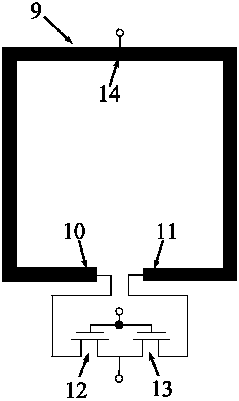
[0038] like image 3 Shown is a schematic diagram of Embodiment 2 of the connection between the antenna and the field effect transistor of the present invention.
[0039] Each of the two ports drawn by the antenna 9 is connected to a field effect transistor, that is, the first port 10 of the antenna 9 is connected to the source of a field effect transistor 12; the second port 11 drawn by the antenna 9 is connected to another field The source of the effect transistor 13; the gates of the two field effect transistors 12 and 13 are connected and loaded with a fixed DC bias voltage; the drains of the two field effect transistors 12 and 13 are connected for outputting detection signals; The position 14 of the neutral line is grounded or loaded with a fixed bias voltage, which is used to provide a direct current path for the field effect transistor.
PUM
 Abstract
Description
Claims
Application Information