On-chip antenna and an antenna array
An on-chip antenna and patch antenna technology, which is applied in the direction of antenna, antenna grounding device, antenna grounding switch structure connection, etc., can solve the problems of difficult setting of antenna unit and CMOS structure, and achieve good engineering realization and high feeding efficiency Effect
- Summary
- Abstract
- Description
- Claims
- Application Information
AI Technical Summary
Problems solved by technology
Method used
Image
Examples
Embodiment 1
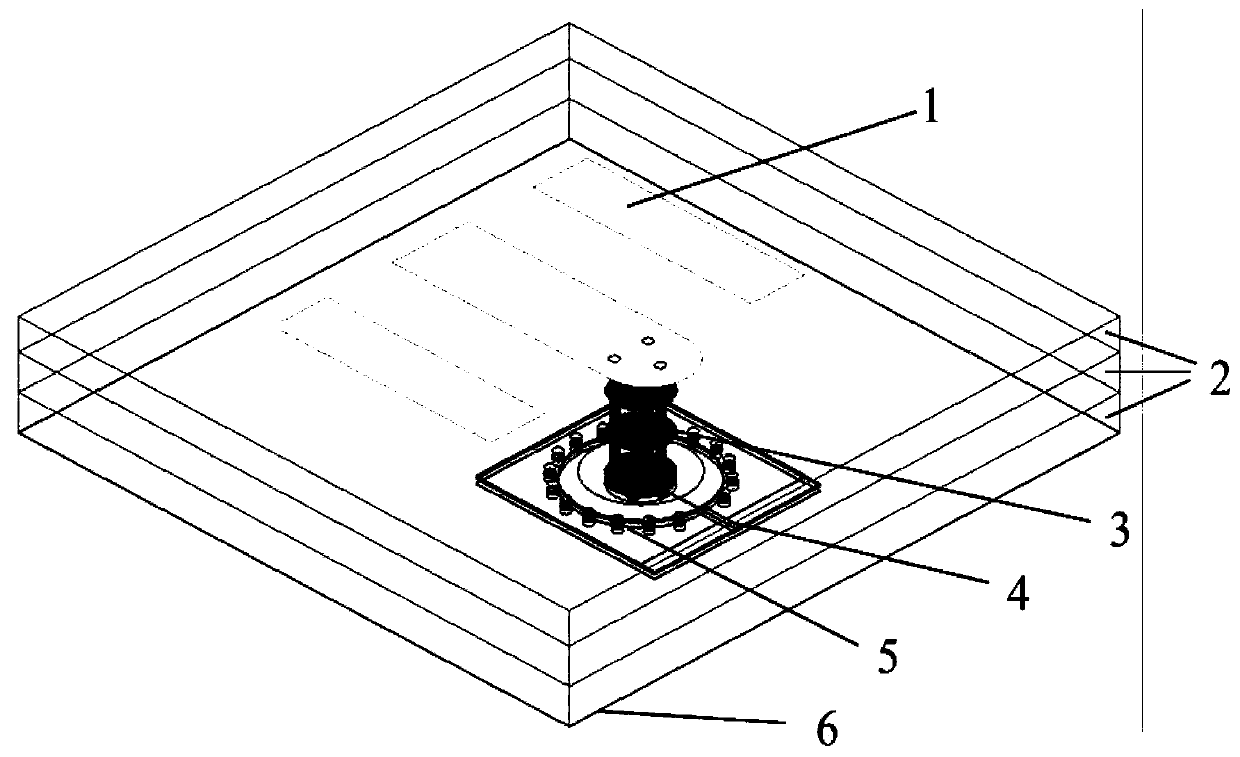
[0022] like figure 1 shown, figure 1 It is a schematic diagram of the three-dimensional structure of the on-chip antenna of the present invention; the on-chip antenna of the present invention includes an antenna substrate 2, a patch antenna unit 1 disposed on the upper surface of the antenna substrate 2, and a CMOS unit disposed on the lower surface of the antenna substrate 2. , the CMOS unit includes a quasi-coaxial feeding structure 5 and a coplanar waveguide feeding structure 4 , and the patch antenna unit 1 is provided with a feeding probe 3 . The feeding probe 3 can be set as a probe metal column 7 distributed in a vertical bundle.
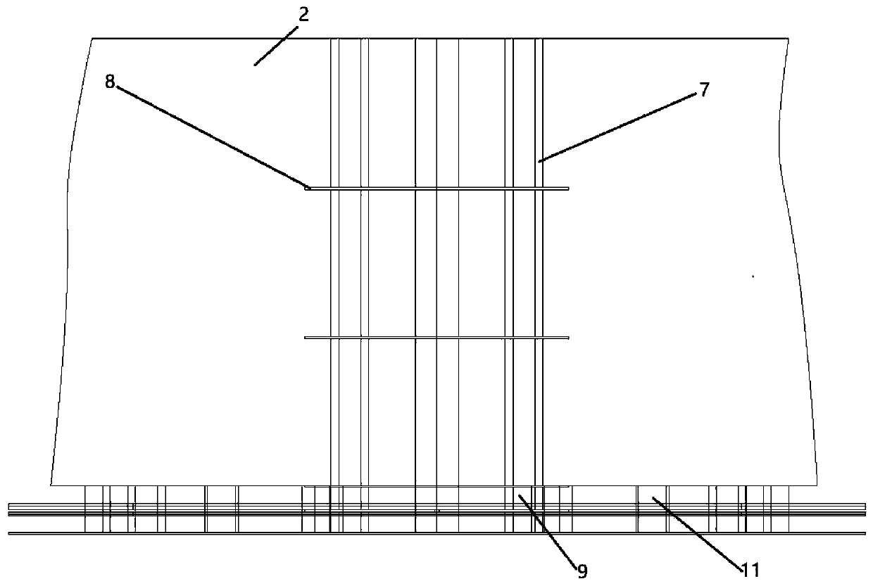
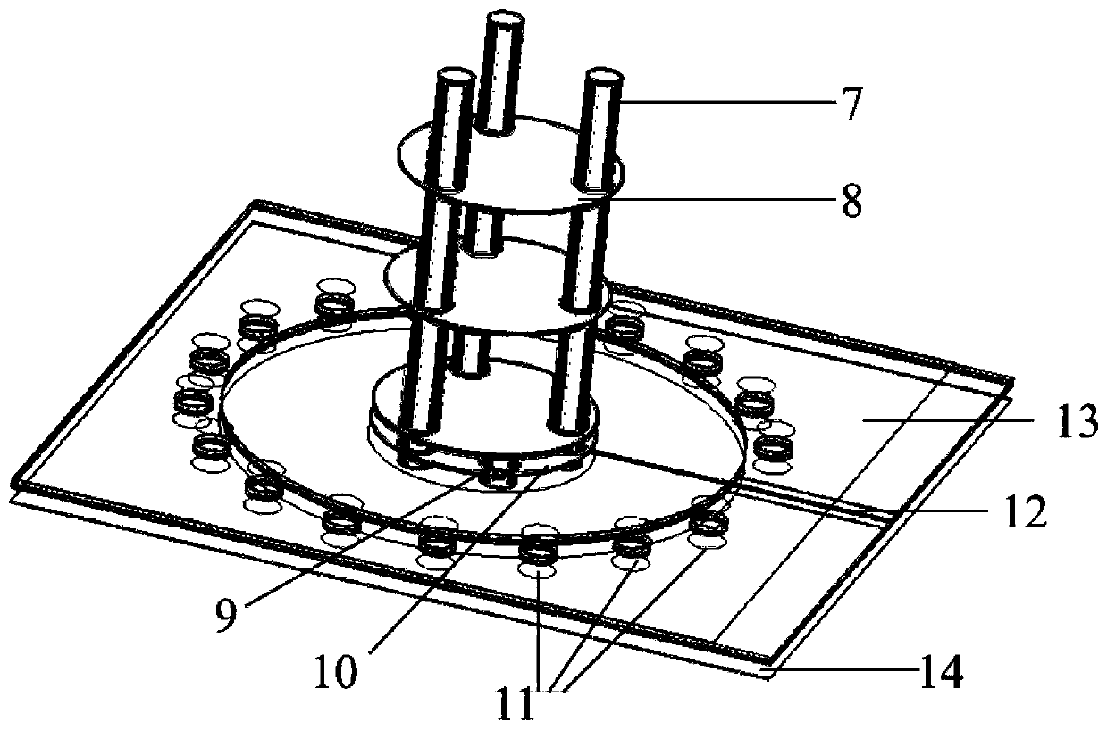
[0023] like figure 2 shown, figure 2 It is a partial cross-sectional view of the on-chip antenna of the present invention; the quasi-coaxial feed structure 5 includes a feed metal column 9 and a fence metal column 11 annularly distributed around the feed metal column 9; the feed metal column 9. The vertical cluster distribution constitu...
Embodiment 2
[0028] The antenna substrate 2 is set as a single-layer dielectric plate; correspondingly, the antenna substrate 2 is a double-sided copper clad laminate. The patch antenna unit 1 in the shape of "chuan" or "mountain" has a circular feed channel etched or etched on the lower surface of the antenna substrate 2, that is, a circular feed channel is provided inside the circular feed channel. Shaped probe metal patch 8 , the probe metal post 7 is connected to the upper surface of the probe metal patch 8 , and the outer copper-clad portion of the annular feed channel serves as the antenna reflection ground 6 .
[0029] The feeding probe 3 can be simply set as a probe metal column 7 at the corresponding position, and the end of the probe metal column 7 corresponds to the connection position with the patch antenna unit 1; When the diameters of the positive electrodes of the electrical probe 3 and the quasi-coaxial feeding structure 5 are relatively large, a plurality of the probe meta...
Embodiment 3
[0031] If the working bandwidth of the antenna is very wide, the antenna substrate 2 can be configured as a dielectric board formed by stacking multiple dielectric layers. Copper clad laminate on the upper surface of the uppermost dielectric layer and etched or etched the patch antenna unit 1 in the shape of "chuan" or "mountain" of the required size, and copper clad laminate on the lower surface of the lowermost dielectric layer The annular feed channel is etched or etched, and other copper-clad areas are used as antenna reflection grounds 6 .
[0032] A number of vertically clustered metal pillar through holes are arranged in the dielectric layer, and the metal pillar through holes are used to install the probe metal pillars 7 , or the metal pillar through holes are filled by a growth process to form the probe metal pillar through holes. At the same time, it is worth noting that the inner wall of the metal column through hole can also be metallized to form a through hole str...
PUM
 Abstract
Description
Claims
Application Information


