Luminous unit coplanar structure of micro light emitting diode display

A technology of micro light-emitting diodes and light-emitting units, which is applied to the light-emitting unit structure of green and green displays, can solve the problems of high production cost of horizontal chips, unfavorable display cost control, and influence on the uniformity of light-emitting units.

Pending Publication Date: 2019-10-29
晶旺半导体(厦门)有限公司
View PDF0 Cites 4 Cited by
  • Summary
  • Abstract
  • Description
  • Claims
  • Application Information

AI Technical Summary

Problems solved by technology

In addition, in terms of the current production technology of micro-LED chips, although horizontal chips are beneficial to flip-chip packaging operations, the production cost of horizontal chips is relatively high, which is not conducive to the cost control of micro-light-emitting diode (LED) displays; especially , in terms of existing red, green and blue LED chips (10, 20, 30), the height of the red LED chip (10) is relatively greater than the height of the green and blue LED chips (20, 30), while the green and blue LED chips The heights of the chips (20, 30) are approximately equal, that is, the height of the relatively large LED chip (such as the red LED chip 10 but not limited) and the remaining LED chips (such as the green and blue LED chips 20 and 30 but not limited) A height difference has been formed between them; therefore when the existing red, green and blue LED chips (10, 20, 30) are packaged on the same plane of the carrier plate 40 (or substrate 1a) of the light-emitting unit 1, from the front as figure 1 The front viewing angle shown), the luminous uniformity of the red, green and blue LED chips (10, 20, 30) is not affected, but it is viewed from an oblique angle (inclined to such as figure 1 As shown in the front viewing angle), because the height of the red LED chip (10) is higher, more red light will be seen, which will affect the uniformity of light emission of the light emitting unit

Method used


Image

  • Luminous unit coplanar structure of micro light emitting diode display
  • Luminous unit coplanar structure of micro light emitting diode display
  • Luminous unit coplanar structure of micro light emitting diode display

Examples


Embodiment Construction

[0023] In order to make the present invention more definite and detailed, the preferred embodiments are listed hereby together with the following diagrams, and the structure and technical characteristics of the present invention are described in detail as follows, wherein each diagram is only used to illustrate the structural relationship and related functions of the present invention , so the size or shape or size of each part is not set according to the actual scale and is not used to limit the present invention:

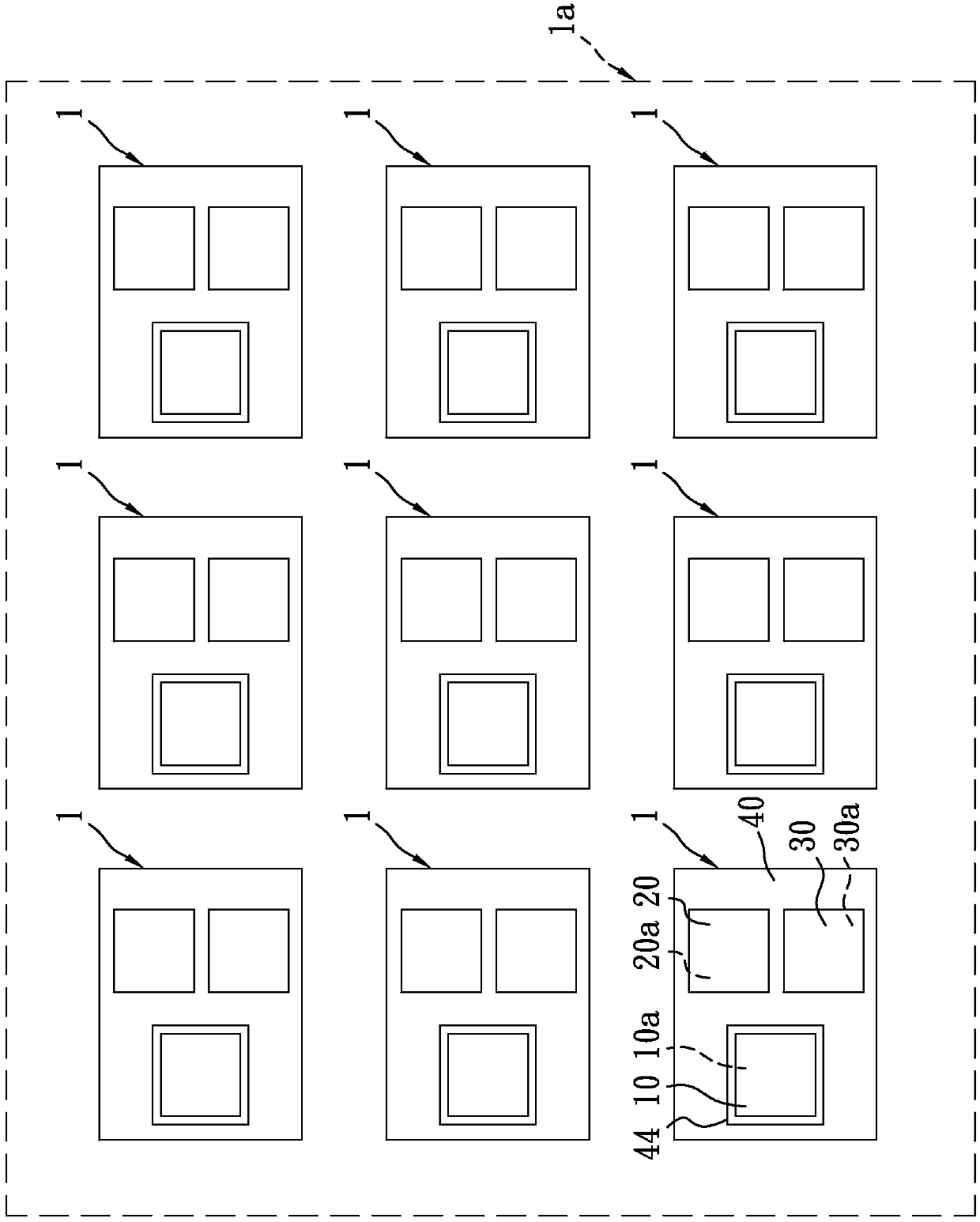
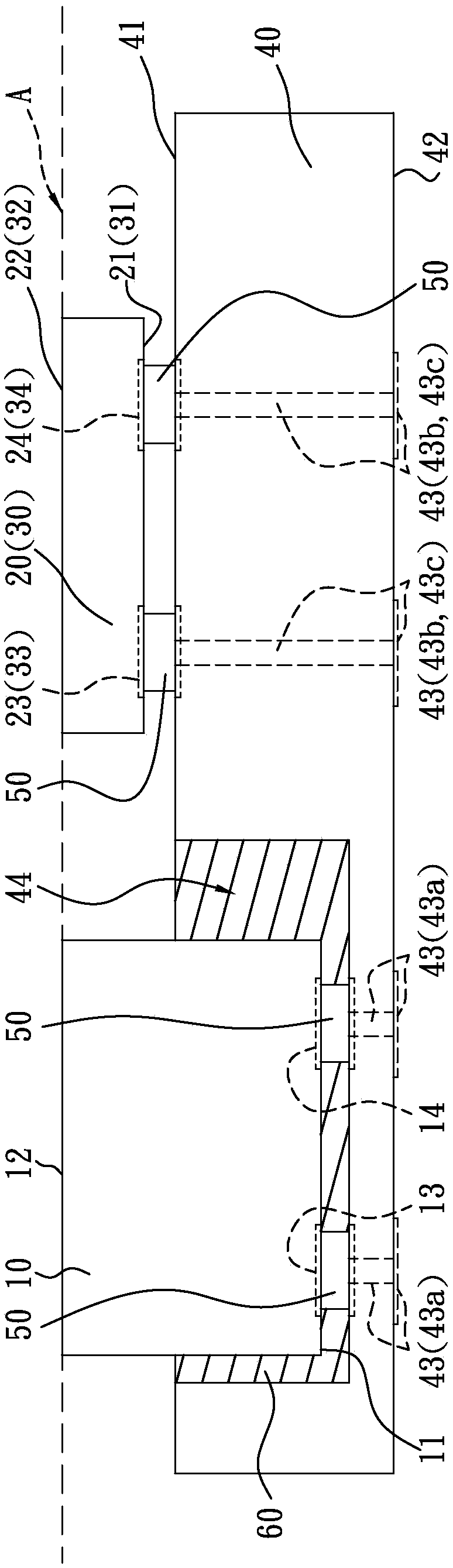
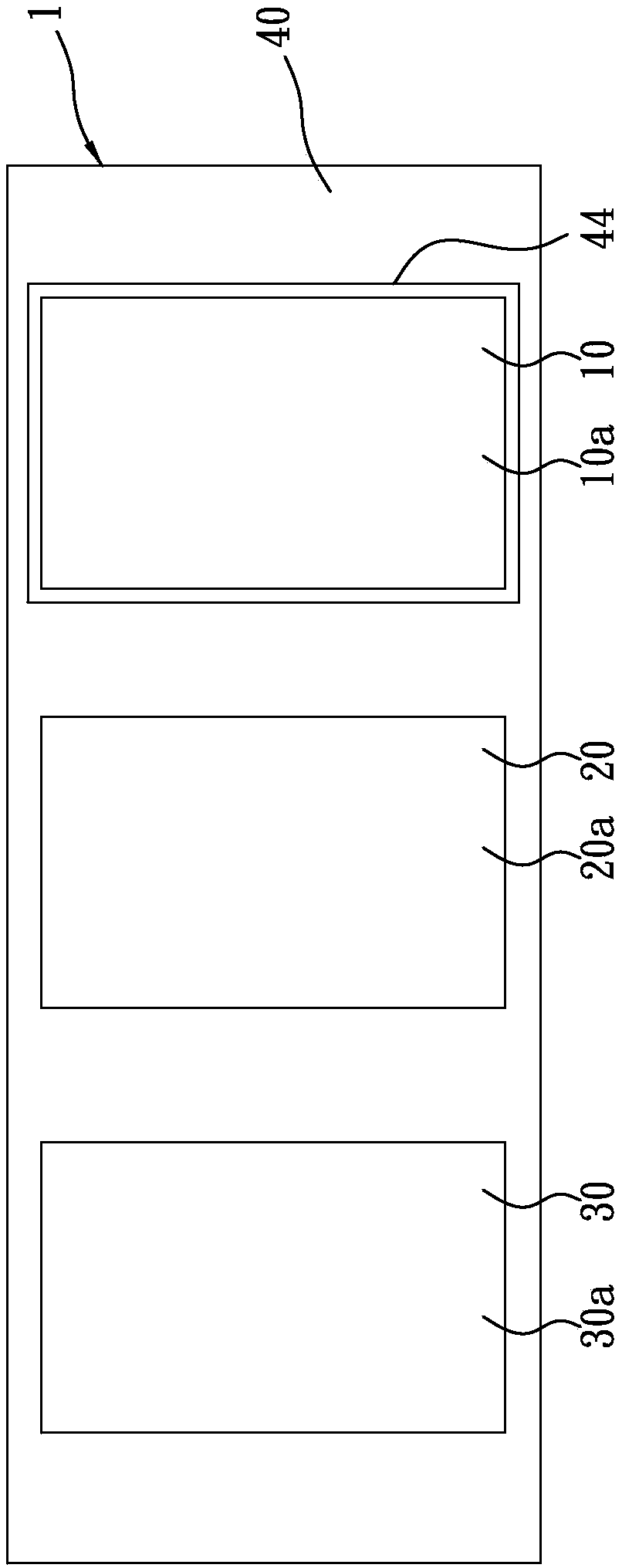
[0024] refer to figure 1 , the micro-light-emitting diode (LED) display of the present embodiment is made up of a plurality of light-emitting units 1 arranged on a substrate (chip) 1a and forming an array, wherein each light-emitting unit 1 (please refer to figure 1 shown in the lower left corner of ) is composed of a red LED chip 10, a green LED chip 20 and a blue LED chip 30 arranged and electrically connected on a carrier board 40, but not limited, for example,...


PUM


Abstract

The invention discloses a luminous unit coplanar structure of a micro light emitting diode display. The micro light emitting diode display is formed through an array which is formed by arranging multiple luminous units on a substrate; the luminous units are formed by arranging red, green and blue LED chips on a support plate; the height of at least one LED chip in the red, green and blue LED chipsincluded by the luminous units is relatively greater than that of other LED chips so that height difference can be formed; the first surface of the support plate is provided with at least one groovefor accommodating the LED chip with relatively large height; and each groove has a depth which is approximately equal to the height difference. Thus, the red, green and blue LED chips can form a coplanar state on the support plate so as to enhance the luminous uniformity of the micro light emitting diode display at different visual angles.

Description

technical field [0001] The invention relates to a light-emitting unit structure of a micro-light-emitting diode display, in particular to a carrier plate on which red, green, and blue LED chips are arranged in the light-emitting unit, at least one groove is provided for accommodating the red, green, and blue LED chips. Among the blue LED chips, the height of the LED chip is relatively large, so that the red, green and blue LED chips can form a coplanar state on the carrier plate to improve the uniformity of light emission of the micro-light-emitting diode display at different viewing angles. Background technique [0002] Micro LED Display (Micro LED Display) is a new generation of display technology. Its structure is a miniaturized LED array, that is, a high-density micro-sized LED array integrated on a substrate (chip), so Micro LED technology can be regarded as LED miniaturization. and matrix technology, and the structural design of the micro-LED display can be regarded as...

Claims


Application Information

Patent Timeline
Patent Type & Authority Applications(China)
IPC IPC(8): H01L27/15
CPCH01L27/156
Inventor 璩泽明庄峰辉
Owner 晶旺半导体(厦门)有限公司
Why Eureka
Try Eureka