Vacuum high-low temperature semiconductor device test probe station and semiconductor device test method

A technology of test probes and test methods, which is applied in the direction of single semiconductor device testing, components and instruments of electrical measuring instruments, etc., can solve the problems of chip implantation Trojan horse structure, hidden safety hazards and high cost, and achieve the effect of stabilizing the test environment.

Pending Publication Date: 2019-11-05
深圳市森美协尔科技有限公司
View PDF21 Cites 10 Cited by
  • Summary
  • Abstract
  • Description
  • Claims
  • Application Information

AI Technical Summary

Problems solved by technology

However, due to the weak foundation of my country's integrated circuit industry, key semiconductor devices mainly rely on imports. Not only are the costs high and the import channels have no quality assurance, but there are also great security risks, such as chips being implanted in Trojan horse structures, etc.

Method used


Image

  • Vacuum high-low temperature semiconductor device test probe station and semiconductor device test method
  • Vacuum high-low temperature semiconductor device test probe station and semiconductor device test method
  • Vacuum high-low temperature semiconductor device test probe station and semiconductor device test method

Examples


Embodiment Construction

[0023] The specific implementation manners of the present invention will be further described in detail below in conjunction with the accompanying drawings and embodiments. The following examples are used to illustrate the present invention, but are not intended to limit the scope of the present invention.

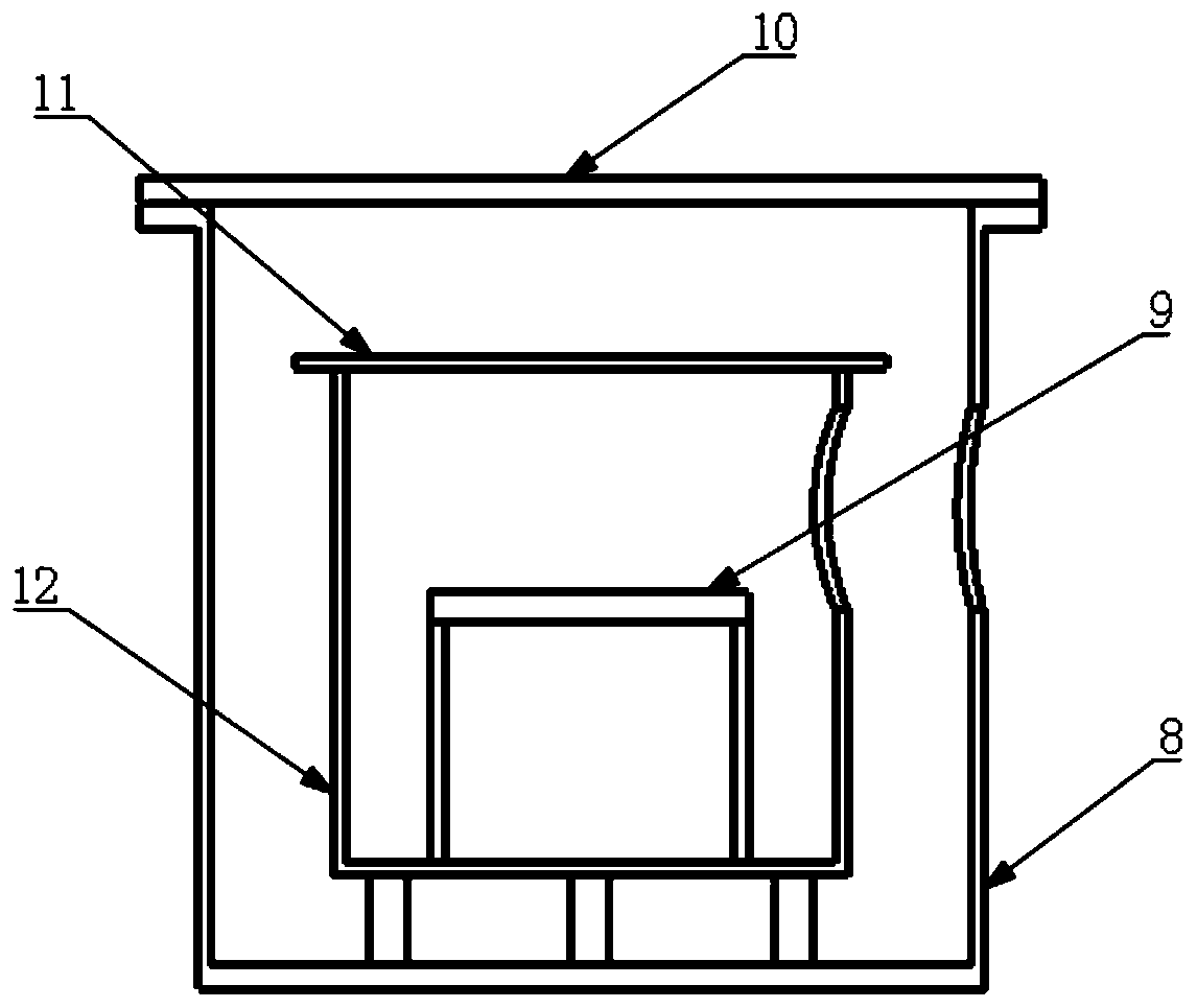
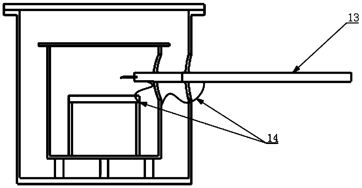
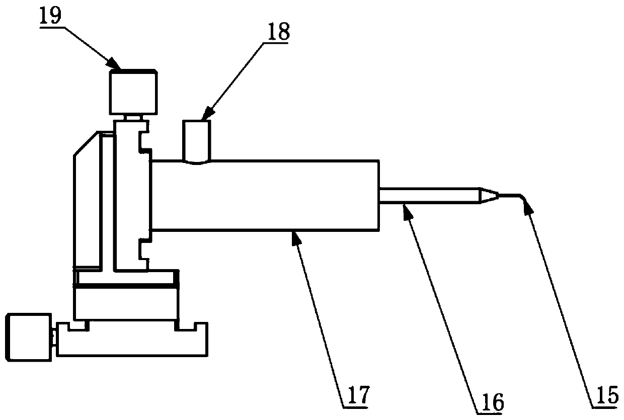
[0024] Such as Figure 1 to Figure 5 As shown, in this embodiment, the vacuum high and low temperature semiconductor device testing probe station includes a vacuum chamber, a radiation shield, a sample stage 9, a probe arm 13, and a microscope.

[0025] The vacuum chamber is used to form a sealed test environment. When simulating a vacuum environment test, a vacuum pump can be used to evacuate the vacuum chamber to form a vacuum environment in the vacuum chamber. In this embodiment, the vacuum chamber includes a vacuum chamber body 8 and a vacuum chamber cover 10 .

[0026] The anti-radiation screen is used to block the radiation from the outside to the sample stage 9, ...


PUM


Abstract

The invention relates to a vacuum high-low temperature semiconductor device test probe station comprising a vacuum cavity, an anti-radiation screen, a sample station and a probe arm; the vacuum cavityis used for forming a sealed test environment; the anti-radiation screen is used for blocking radiation of the outside to the sample station and is located in the vacuum cavity; the sample station isused for containing a sample and located in the anti-radiation screen; the probe arm comprises a probe needle rod and a probe located at the tail end of the probe needle rod; and the probe needle rodpenetrates through the vacuum cavity and the anti-radiation screen, so that the probe stretches into the position where the sample is located so as to conduct point needling. The invention further discloses a semiconductor device test method. The vacuum high-low temperature semiconductor device test probe station as mentioned above is used. According to the vacuum high-low temperature semiconductor device test probe station and the semiconductor device test method provided by the invention, the structures such as the vacuum cavity, the anti-radiation screen and the like are arranged, so thata test environment integrated with high temperature, low temperature, vacuum and the like can be effectively created, and a stable test environment can be provided for the produced semiconductor device.

Description

technical field [0001] The invention relates to the technical field of semiconductor device testing, in particular to a vacuum high-low temperature semiconductor device testing probe station and a semiconductor device testing method. Background technique [0002] With the development of aerospace technology, some highly reliable and high-performance semiconductor devices, especially core aerospace devices, have become an important symbol to measure the level of a country's aerospace technology. However, due to the weak foundation of my country's integrated circuit industry, key semiconductor devices mainly rely on imports. Not only are the costs high and the import channels have no quality assurance, but there are also great security risks, such as chips being implanted in Trojan horse structures. To this end, it is necessary to have core devices developed by itself. [0003] However, in every research and development process, in order to ensure that the device can withstan...

Claims


Application Information

Patent Timeline
Patent Type & Authority Applications(China)
IPC IPC(8): G01R31/26G01R1/04G01R1/067G01R1/18
CPCG01R1/04G01R1/06705G01R1/18G01R31/2601
Inventor 刘世文范玉祥
Owner 深圳市森美协尔科技有限公司
Why Eureka
Try Eureka