
PMOS device stress layer structure and formation method thereof

A stress layer and device technology, applied in the fields of semiconductor devices, semiconductor/solid-state device manufacturing, electrical components, etc., can solve problems such as the decline of electrical properties of devices, and achieve the effect of reducing volume difference, improving electrical properties, and accelerating growth rate.

Pending Publication Date: 2019-11-05
SEMICON MFG INT (SHANGHAI) CORP +1
View PDF5 Cites 0 Cited by
  • Summary
  • Abstract
  • Description
  • Claims
  • Application Information

AI Technical Summary

Problems solved by technology

For example, PMOS devices, due to the different volumes of the stress layer formed in the trenches at different positions, the electrical performance of the final device is reduced

Method used


Image

  • PMOS device stress layer structure and formation method thereof
  • PMOS device stress layer structure and formation method thereof
  • PMOS device stress layer structure and formation method thereof

Examples


Embodiment Construction

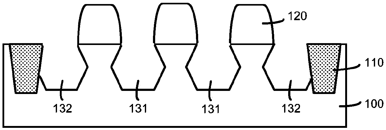
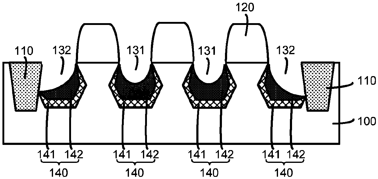
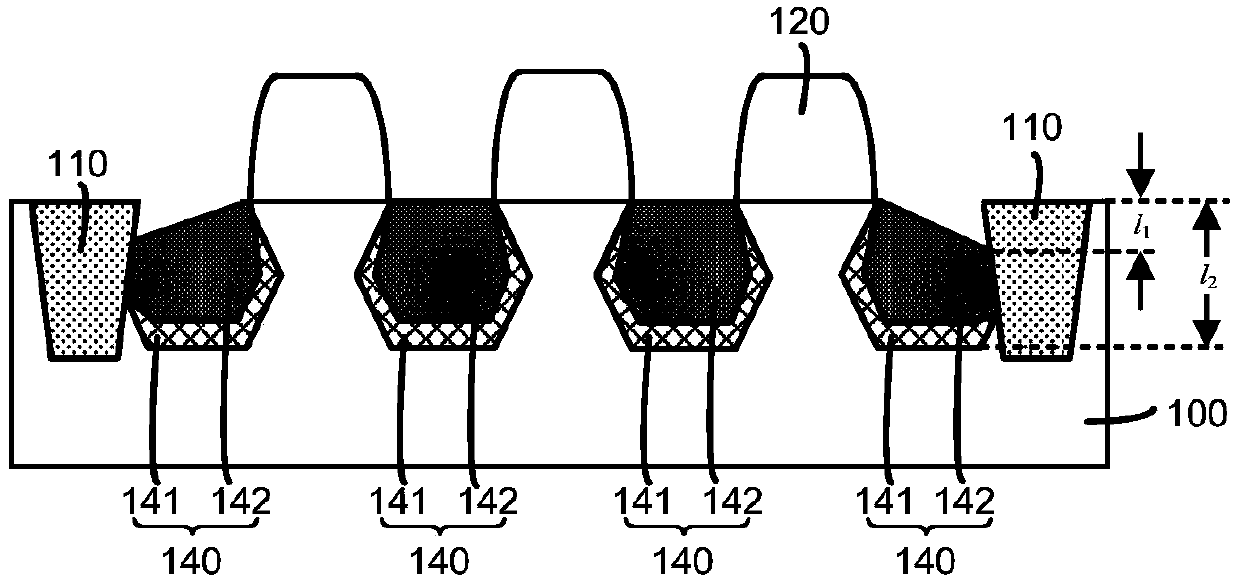
[0027] As mentioned above, in the existing PMOS devices, there is a problem of large volume difference of the stress layer at different positions, which further affects the performance of the semiconductor device.

[0028] After research, it is found that the reason for the above problems is: when forming the stress layer of the PMOS device, the growth rate of SiGe between the gate structure and the shallow trench isolation structure is relatively slow, and the growth is easy to stop at the crystal plane of SiGe. Finally, the volume of the stress layer here is smaller.

[0029] In order to solve this problem, the present invention provides a method for forming the stress layer structure of a PMOS device. When the SiGe between the gate structure and the shallow trench isolation structure stops growing on the crystal plane of SiGe, heat treatment is performed to destroy The crystal plane of SiGe continues to grow.

[0030] Various exemplary embodiments of the present inventi...


PUM


Abstract

The invention discloses a formation method of a PMOS device stress layer structure. The formation method comprises the following steps ofproviding a semiconductor substrate, shallow groove isolation structures and gate structures, wherein the gate structures are arranged on the semiconductor substrate at intervals; forming grooves in the semiconductor substrate, wherein the grooves comprise firstgrooves and second grooves, each first groove is formed between every two adjacent gate structures, and the second grooves are formed between the gate structures and the shallow groove isolation structures; using a first technology to form stress layers inside the grooves; when the stress layers formed in the second grooves grow to a certain crystal face of a material used in the stress layer, carrying out heat treatment on the stress layers inside the grooves; and using a second technology to form stress layers inside the grooves continuously. The volume difference of the stress layers at different positions is reduced, and the performance of a semiconductor device is improved.

Description

technical field [0001] The invention relates to the field of semiconductor manufacturing, in particular to a PMOS device stress layer structure and a forming method thereof. Background technique [0002] During the fabrication of MOS devices, a stress layer is formed between adjacent gate structures to apply stress to the channel. In order to effectively utilize the semiconductor substrate and improve the integration level of the circuit, a trench is usually formed between the gate structure and the shallow trench isolation structure, and further a stress layer is also formed. For example, in PMOS devices, due to the different volumes of stress layers formed in trenches at different positions, the electrical performance of the final device is reduced. [0003] Therefore, there is an urgent need for a method for forming a PMOS stress layer structure that improves the electrical performance of semiconductor devices. Contents of the invention [0004] The embodiment of the ...

Claims


Application Information

Patent Timeline
Patent Type & Authority Applications(China)
IPC IPC(8): H01L29/78H01L21/336H01L29/06
CPCH01L29/78H01L29/66477H01L29/06
Inventor 罗康汪军
Owner SEMICON MFG INT (SHANGHAI) CORP
Learn More