Pixel circuit, display panel and display equipment

A pixel circuit and level technology, applied in the field of display equipment, can solve problems such as high cost, large area occupied by pixel circuits, unfavorable narrow frame design, etc., and achieve the effect of reducing cost, reducing layout space, and realizing narrow frame of products

Pending Publication Date: 2019-11-12
BOE TECH GRP CO LTD +1
View PDF8 Cites 5 Cited by
  • Summary
  • Abstract
  • Description
  • Claims
  • Application Information

AI Technical Summary

Problems solved by technology

Depend on image 3 and Figure 4 It can be seen that both G1 and G2 need to be scanned line by line during the scanning (Scan) period, which leads to an excessively large area occupied by the pixel circuit (requiring double driving signals), which is not conducive to the realization of a narrow frame design of the product, and the cost is high

Method used


Image

  • Pixel circuit, display panel and display equipment
  • Pixel circuit, display panel and display equipment
  • Pixel circuit, display panel and display equipment

Examples


Embodiment Construction

[0037] Embodiments of the present invention are described in detail below, examples of which are shown in the drawings, wherein the same or similar reference numerals designate the same or similar elements or elements having the same or similar functions throughout. The embodiments described below by referring to the figures are exemplary and are intended to explain the present invention and should not be construed as limiting the present invention.

[0038] A pixel circuit, a display panel, and a display device according to embodiments of the present invention will be described below with reference to the accompanying drawings.

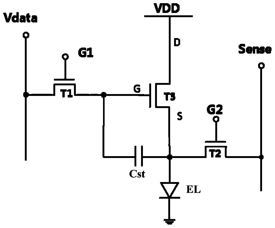
[0039] Figure 5 is a structural diagram of a pixel circuit according to an embodiment of the present invention. Such as Figure 5 As shown, the circuit includes: a first transistor T1, a light emitting unit EL, a second transistor T2, a third transistor T3, a fourth transistor T4 and a capacitor Cst.

[0040] Wherein, the first pole of ...


PUM


Abstract

The invention discloses a pixel circuit, a display panel and display equipment, and the pixel circuit comprises a first transistor, a second transistor, a third transistor, a fourth transistor, a fifth transistor, a sixth transistor and a seventh transistor, a light emitting unit; the first pole of the second transistor is connected with the anode of the light-emitting unit, the second pole is used for inputting reference voltage, and the control pole is used for inputting first driving signals; a third transistor; a first electrode of the fourth transistor is connected with the data line, a second electrode is connected with the anode of the light-emitting unit, and a control electrode is used for inputting a second driving signal; and a capacitor connected between the control electrode of the third transistor and the second electrode of the third transistor. According to the pixel circuit, one-to-one voltage compensation is carried out on the driving transistors through the data lines, the compensation function is effectively optimized, the product yield is improved, line-by-line displacement design does not need to be carried out on the second driving signals, the layout space occupied by the pixel circuit is greatly reduced, and therefore the narrow bezel of a product can be achieved, and the cost can be reduced.

Description

technical field [0001] The present invention relates to the field of display technology, in particular to a pixel circuit, a display panel, and a display device. Background technique [0002] AMOLED (Active-matrix organic light-emitting diode, active-matrix organic light-emitting diode) is expected to replace liquid crystal and become the mainstream choice for next-generation displays due to its high contrast ratio, wide viewing angle and fast response speed. Generally, in the pixel circuit design of OLED (Organic Light-Emitting Diode, Organic Light-Emitting Diode) products, considering the limitations of the process, all pixel circuits are designed using N-type TFT (Thin Film Transistor, thin film transistor), such as 54.5inch AMOLED panel design , which uses as figure 1 In the 3T1C pixel circuit shown, T1-T3 are the first to third transistors, Vdata is the data line, VDD is the DC power supply, Sense is the sensing line, EL is the light emitting unit, G1 is the first driv...

Claims


Application Information

Patent Timeline
Patent Type & Authority Applications(China)
IPC IPC(8): G09G3/3291G09G3/3258G09G3/3208
CPCG09G3/3208G09G3/3258G09G3/3291
Inventor 袁志东李永谦袁粲焦超
Owner BOE TECH GRP CO LTD
Why Eureka
Try Eureka