Array substrate and display device

An array substrate and substrate technology, applied in semiconductor devices, electrical components, circuits, etc., can solve problems such as uneven light-emitting surface of the light-emitting layer, inability to planarize the double-layer SD wiring structure, and affect the display effect of the display device, etc., to achieve improved Screen display effect, enhance user experience, and prevent level difference

Active Publication Date: 2019-11-15
WUHAN CHINA STAR OPTOELECTRONICS SEMICON DISPLAY TECH CO LTD
View PDF4 Cites 3 Cited by
  • Summary
  • Abstract
  • Description
  • Claims
  • Application Information

AI Technical Summary

Problems solved by technology

[0005] The object of the present invention is to provide an array substrate and a display device to solve the problem of uneven light-emitting surface of the light-emitting layer caused by the inability to planarize the double-layer SD wiring structure in the prior art, thereby affecting the display effect of the display device

Method used


Image

  • Array substrate and display device
  • Array substrate and display device

Examples


Embodiment Construction

[0033] The following describes the preferred embodiments of the present invention with reference to the accompanying drawings to prove that the present invention can be implemented. The embodiments of the invention can fully introduce the present invention to those skilled in the art, making its technical content clearer and easier to understand. The present invention can be embodied by many different forms of invention embodiments, and the protection scope of the present invention is not limited to the embodiments mentioned herein.

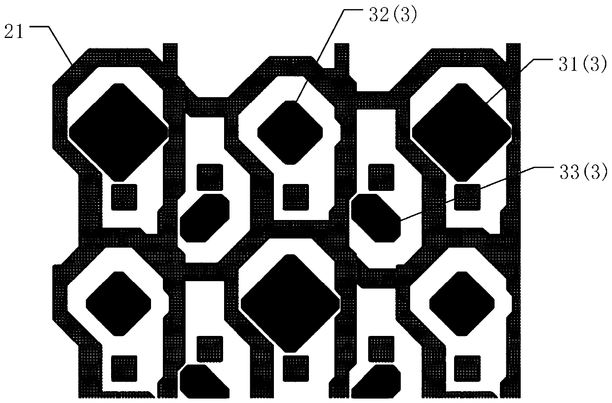
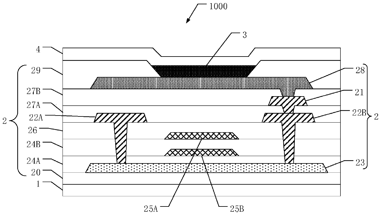
[0034] In the drawings, components with the same structure are denoted by the same numerals, and components with similar structures or functions are denoted by similar numerals. The size and thickness of each component shown in the drawings are arbitrarily shown, and the present invention does not limit the size and thickness of each component. In order to make the illustration clearer, the thickness of parts is appropriately exaggerated in some ...


PUM


Abstract

The invention provides an array substrate and a display device. The array substrate includes a substrate, a thin film transistor structure layer and a light emitting layer. The thin film transistor structure layer is arranged on the substrate, and the thin film transistor structure layer has a number of wires. The light emitting layer is arranged on the thin film transistor structure layer, and the light emitting layer has a number of light emitting units. The projection of the wires on the substrate avoids the projection of the light emitting unit on the substrate.

Description

technical field [0001] The invention relates to the field of display technology, in particular to an array substrate and a display device. Background technique [0002] In the field of display technology, flat panel display devices such as Liquid Crystal Display (LCD) and Organic Light-Emitting Diode (OLED) have gradually replaced cathode line tube displays. Among them, OLED display panels gradually gain the upper hand due to their unique advantages such as low power consumption, high saturation, fast response time and wide viewing angle, and will have broad application space in vehicles, mobile phones, tablets, computers and TV products in the future. [0003] The mainstream driving method of OLED display panels is current drive, and the working current is transmitted from the lower border of the display panel through the source drain (SD: Source Drain). Because the source drain itself has a certain resistance, there is a voltage drop (IRDrop) phenomenon in signal transmiss...

Claims


Application Information

Patent Timeline
Patent Type & Authority Applications(China)
IPC IPC(8): H01L27/32
CPCH10K59/1213H10K59/131H10K59/352H10K59/353H10K59/123H10K59/124H10K59/121H10K50/844H10K59/122
Inventor 周思思
Owner WUHAN CHINA STAR OPTOELECTRONICS SEMICON DISPLAY TECH CO LTD
Why Eureka
Try Eureka