Display panel preparation method, display panel and display device
A display panel, directly above technology, applied in the field of display devices, can solve problems such as damage to the array film layer and difficulties in yield improvement, and achieve the effects of ensuring packaging effects, improving packaging effects, and improving display effects
- Summary
- Abstract
- Description
- Claims
- Application Information
AI Technical Summary
Problems solved by technology
Method used
Image
Examples
preparation example Construction
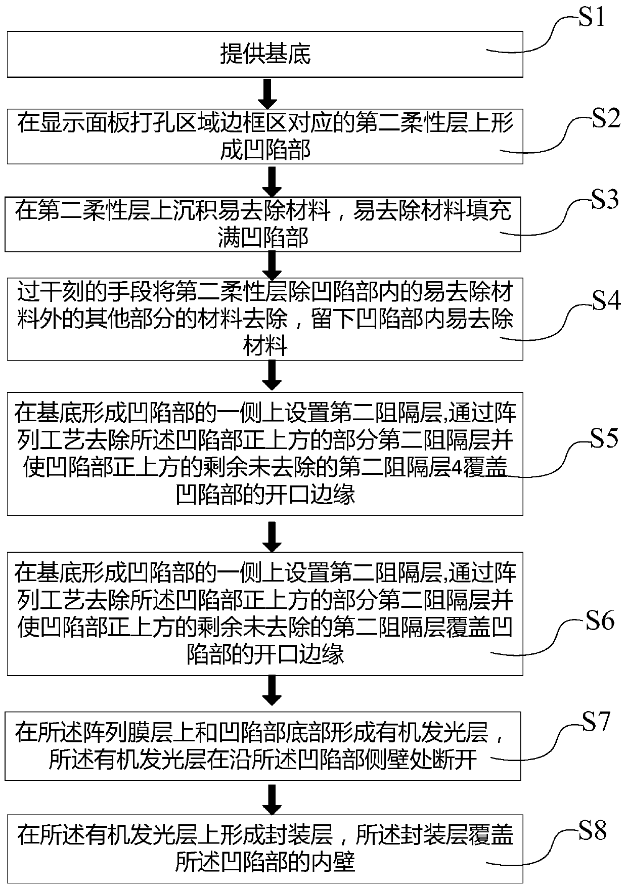
[0042] Such as figure 1 As shown, the preparation method of the display panel provided by the present invention includes the following steps:
[0043] A substrate is provided, wherein the substrate comprises a first flexible layer 1, a first barrier layer 2 and a second flexible layer 3;
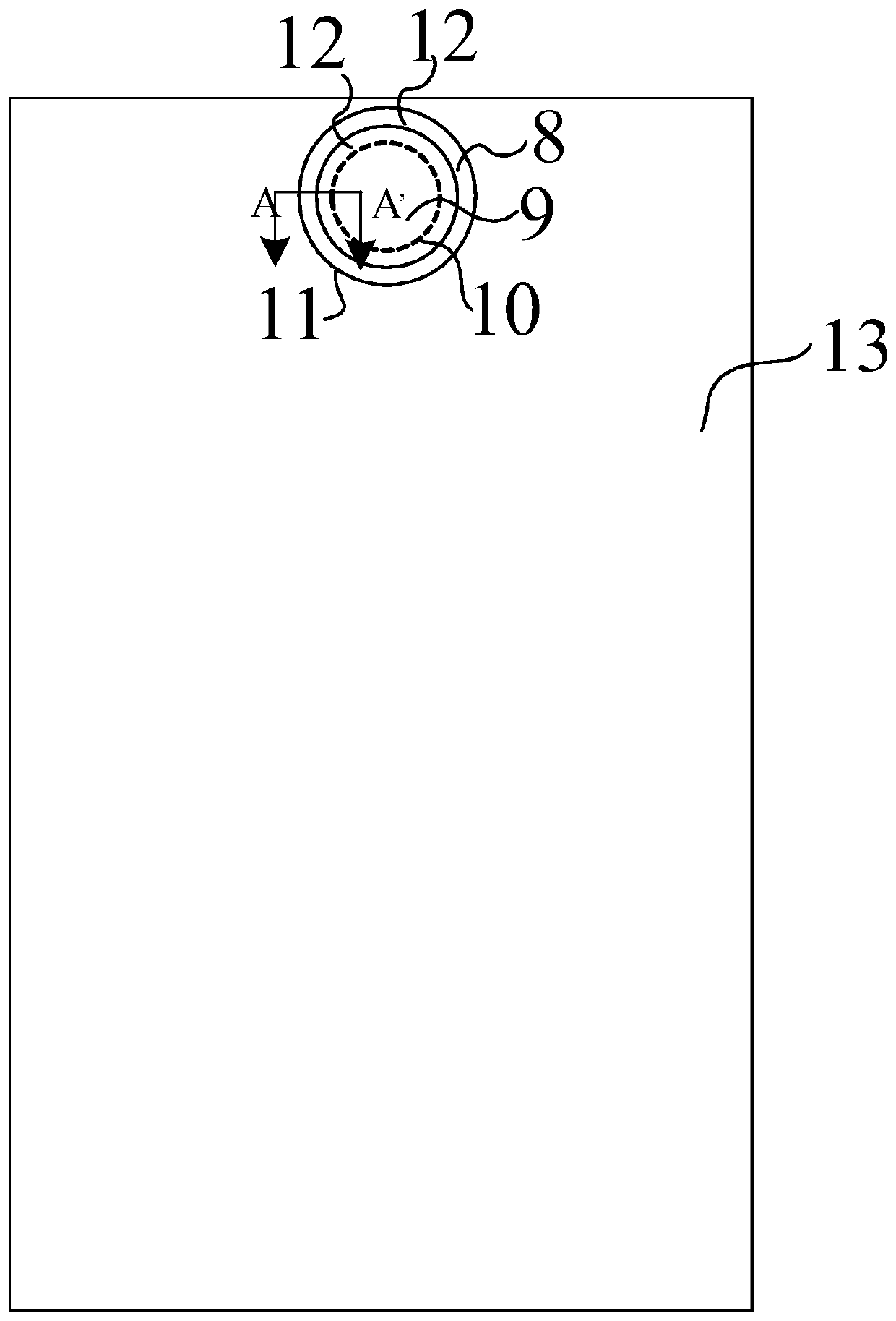
[0044] A recessed portion 12 is formed on the substrate corresponding to the frame area of the perforated area of the display panel, and the recessed portion 12 is filled with easy-to-remove materials; specifically, the perforated area of the display panel can be correspondingly provided with a camera, an earpiece, or a physical button, etc. External components; along the direction of increasing radius in the frame area, the recesses are arranged at intervals, the number can be selected according to needs, for example, it can be 1, 4 or 10, and the shape can be circular, elliptical or other; The depressions 12 formed on the circles surrounded by different radii jointly form a ring alo...
Embodiment 1
[0068] This embodiment provides a method for preparing a display panel, such as figure 1 and 3 shown, including the following steps:
[0069] S1. Provide a base, the base includes a first flexible layer 1, a first barrier layer 2 and a second flexible layer 3 which are sequentially stacked, the first flexible layer 1 and the second flexible layer 3 are both polyimide layers, the first The thickness of the flexible layer 1 is 10 μm, the thickness of the second flexible layer 3 is 10 μm; the first barrier layer 2 is an inorganic layer, the inorganic layer is a silicon nitride (SiNx) layer, and the thickness of the first barrier layer 2 is 1 μm;
[0070] S2. Form a depression on the substrate corresponding to the frame area of the perforated area of the display panel. The depression is arranged on the second flexible layer 3. The depression can specifically be an annular depression. The annular depression has an annular depression groove. The part is formed by means of expo...
Embodiment 2
[0081] This embodiment provides a method for preparing a display panel, such as figure 1 and 3 shown, including the following steps:
[0082] S1. Provide a base, the base includes a first flexible layer 1, a first barrier layer 2, and a second flexible layer 3 that are stacked in sequence, and both the first flexible layer 1 and the second flexible layer 3 are polyimide layers. The difference in the thickness of each film layer of the substrate in Example 1 is that the thickness of the first flexible layer 1 is 8 μm, and the thickness of the second flexible layer 3 is 12 μm; the first barrier layer 2 is an inorganic layer, and the inorganic layer is silicon nitride (SiNx ) layer, the thickness of the first barrier layer 2 is 0.8 μm;
[0083] S2. Form a depression on the substrate corresponding to the frame area of the perforated area of the display panel. The depression is arranged on the second flexible layer 3. The depression can specifically be an annular depression. ...
PUM
 Abstract
Description
Claims
Application Information


