Inverted image enhanced ultrafast imaging detector

An imaging detector and image enhancement technology, which is applied to the detailed information of electron multipliers, instruments, dynodes, etc., can solve the problems of semiconductor chips that are prone to vacuum breakdown, so as to avoid the risk of vacuum breakdown, high electron incident energy and space Effects of resolution characteristics, improved detection sensitivity, and time-space resolution characteristics

Inactive Publication Date: 2019-11-22
XI'AN INST OF OPTICS & FINE MECHANICS - CHINESE ACAD OF SCI
View PDF5 Cites 2 Cited by
  • Summary
  • Abstract
  • Description
  • Claims
  • Application Information

AI Technical Summary

Problems solved by technology

[0007] The present invention combines cascade inverted low-light image enhancement technology and all-optical solid-state ultrafast diagnosis technology, overcomes the problem that semiconductor chips are easy to break down in vacuum in the existing double close-fitting structure, and fully uti

Method used


Image

  • Inverted image enhanced ultrafast imaging detector
  • Inverted image enhanced ultrafast imaging detector

Examples


Embodiment Construction

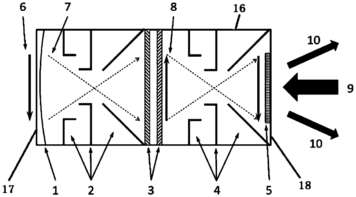
[0034] In order to make the purpose, advantages and features of the present invention clearer, an inverted image-enhanced ultrafast imaging detector proposed by the present invention will be further described in detail below with reference to the accompanying drawings and specific embodiments. Advantages and features of the present invention will be apparent from the following description and claims. It should be noted that: the drawings are all in a very simplified form and use inaccurate proportions, which are only used to facilitate and clearly illustrate the purpose of the embodiments of the present invention; secondly, the structures shown in the drawings are often actual structures part; again, each drawing needs to display different emphasis points, and sometimes adopts different scales.

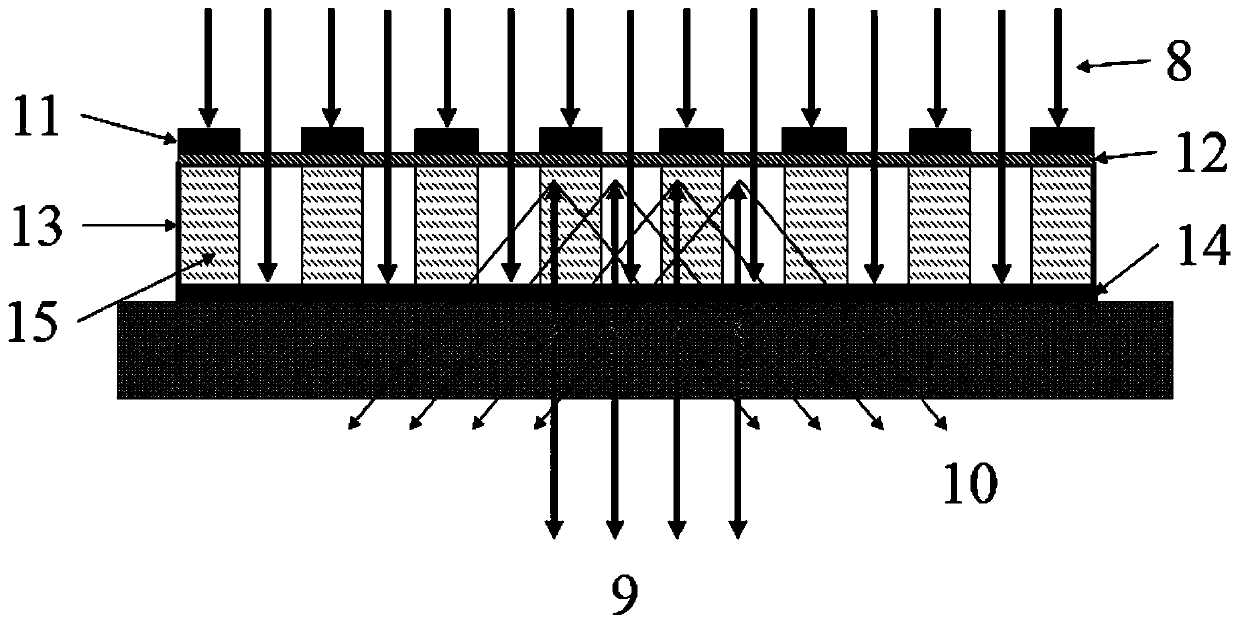
[0035] The specific structure of the inverted image-enhanced ultrafast imaging detector provided in this embodiment can be found in figure 1 : Concretely include casing 16, input win...


PUM

PropertyMeasurementUnit
Thicknessaaaaaaaaaa
Thicknessaaaaaaaaaa
Thicknessaaaaaaaaaa

Abstract

The invention relates to an inverted image enhanced ultrafast imaging detector, and solves the problem that a semiconductor chip in an existing double-near-surface-mount structure is prone to vacuum breakdown. The detector comprises a shell, an input window, an output window, a photoelectric cathode, a first electrostatic focusing electrode, a micro-channel plate, a second electrostatic focusing electrode and a semiconductor detection chip, an input window and an output window are arranged at the two ends of the shell respectively. The inner surface of the input window is plated with a layer of conductive film, and the photoelectric cathode is manufactured on the conductive film; the semiconductor detection chip clings to the inner surface of the output window; a first electrostatic focusing electrode, a micro-channel plate and a second electrostatic focusing electrode are sequentially arranged between the photoelectric cathode and the semiconductor detection chip; the first electrostatic focusing electrode and the second electrostatic focusing electrode are the same; and the input surface and the output surface of the micro-channel plate are loaded with the working voltage.

Description

technical field [0001] The invention relates to the technical field of ultrafast diagnosis, in particular to an inverted image-enhanced ultrafast imaging detector. Background technique [0002] The development of ultra-fast diagnostic technology has extremely important scientific significance for the research in the fields of energy, materials, biology, photophysics, photochemistry, intense light physics and high-energy physics, and is a necessary condition for human beings to expand their cognitive fields and achieve original innovations. Instruments and equipment associated with ultra-fast diagnostic technology are indispensable research tools and means in frontier science and cutting-edge technology. [0003] Traditional high-speed diagnostic equipment includes high-speed image intensification CCD, high-speed gated framing camera, traveling wave gated framing camera, streak camera, etc. [0004] Among them, the streak camera can achieve time resolution of one-dimensional...

Claims


Application Information

Patent Timeline
IPC IPC(8): G01N21/64H01J43/06
CPCG01N21/6408H01J43/06
Inventor 田进寿何凯高贵龙汪韬闫欣辛丽伟李少辉尹飞韦永林徐向晏卢裕王兴刘虎林陈萍温文龙王超王俊峰赛小锋
Owner XI'AN INST OF OPTICS & FINE MECHANICS - CHINESE ACAD OF SCI
Why Eureka
Try Eureka