

A fan-out chip packaging structure and packaging method
A chip packaging structure and chip packaging technology, applied in the direction of semiconductor/solid-state device components, semiconductor devices, electrical components, etc., can solve the problems of low reliability of the packaging structure, stress fracture failure, etc. Reduced shear stress and improved reliability
- Summary
- Abstract
- Description
- Claims
- Application Information
AI Technical Summary
Problems solved by technology
Method used
Image

Examples
Embodiment 1
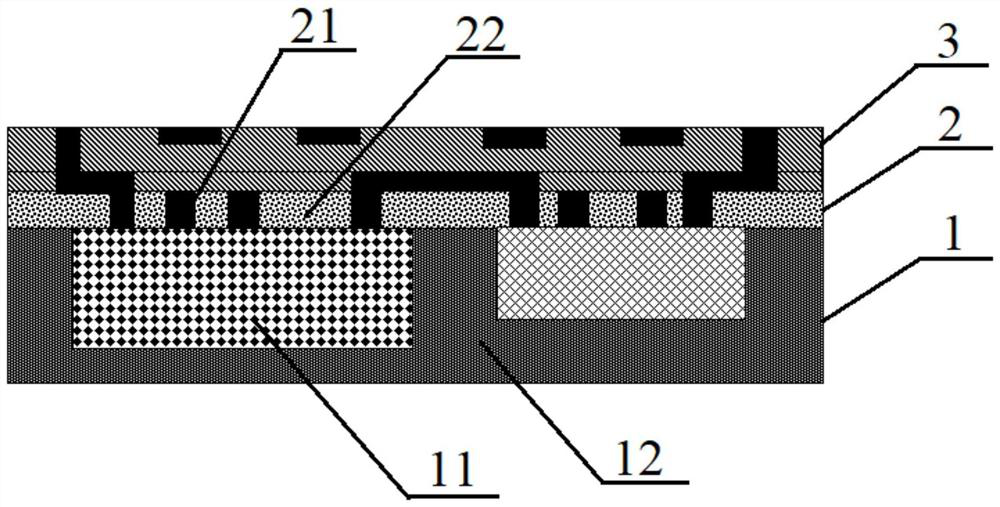
[0030] This embodiment provides a fan-out chip packaging structure, such as figure 1 As shown, the packaging structure includes: a plastic package body 1 , an interconnection layer 2 and a redistribution layer 3 .
[0031] Such as figure 1 As shown, at least one chip 11 is packaged inside the plastic package 1 , and the device surface of the chip 11 is exposed outside the plastic package 1 . Here, the device surface of the chip 11 refers to the surface where the pads of the chip 11 are located. Specifically, the chip 11 can be first mounted on the substrate 4 according to the direction that the device surface of the chip 11 faces the substrate 4, and then mounted on the substrate 4. The molding compound is injected to form the molding layer 12 that encapsulates five surfaces of the chip 11 except the device surface, and then the molding layer 12 and the chip 11 are peeled off from the substrate 4 to form the molding body 1 .
[0032] Such as figure 1 As shown, the interconn...
Embodiment 2
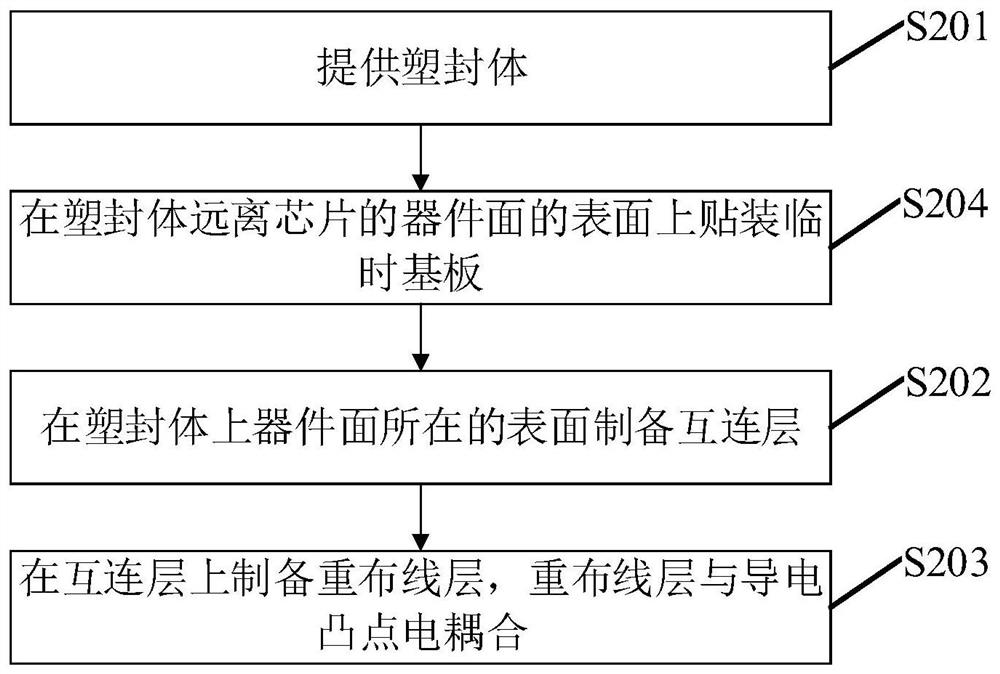
[0040] This embodiment provides a fan-out chip packaging method, and the packaging structure in Embodiment 1 can be prepared according to the method and its preferred implementation, and what has been explained will not be repeated.
[0041] The fan-out chip packaging method provided in this embodiment, such as figure 2 shown, including the following steps:
[0042] S201: Provide a plastic package.
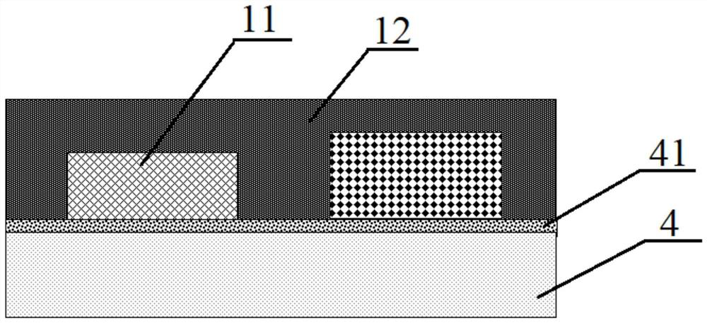
[0043] here, as image 3 As shown, at least one chip 11 is packaged inside the plastic package 1 , and the device surface of the chip 11 is exposed outside the plastic package 1 .
[0044] Specifically, such as image 3 As shown, the plastic package 1 can be prepared by the following steps:
[0045] Step A1: pasting a first temporary bonding glue 41 on a substrate 4 .
[0046] Step A2: paste the chip 11 on the first temporary bonding glue 41 according to the direction that the device surface of the chip 11 faces the first temporary bonding glue 41 .
[0047] Step A3: dispos...
PUM
 Abstract
Description
Claims
Application Information