
A display substrate, its preparation method, and a display device

A display substrate and display area technology, which is applied in semiconductor/solid-state device manufacturing, semiconductor devices, electrical components, etc., can solve problems such as prone to short circuit and affect the overall yield of the screen, so as to reduce the risk of short circuit, excellent blocking effect, The blocking effect is more effective

Active Publication Date: 2021-12-10
BOE TECH GRP CO LTD +1
View PDF0 Cites 0 Cited by
  • Summary
  • Abstract
  • Description
  • Claims
  • Application Information

AI Technical Summary

Problems solved by technology

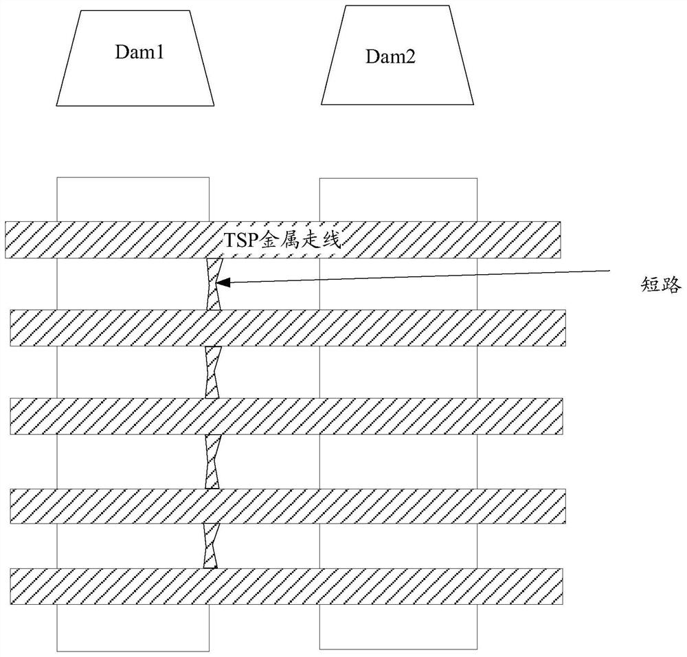
[0002] In the active matrix organic light emitting diode (Active Matrix Organic Light Emitting Diode, AMOLED) display substrate, the IC (Integrated Circuit, integrated circuit) area has a touch screen wiring horizontal DAM structure, which is prone to short circuit. There are many short-circuit problems in the touch screen traces where the IC crosses the DAM, which affects the overall yield of the screen.

Method used


Image

  • A display substrate, its preparation method, and a display device
  • A display substrate, its preparation method, and a display device
  • A display substrate, its preparation method, and a display device

Examples


Embodiment Construction

[0034] In order to make the purpose, technical solution and advantages of the present invention more clear, the embodiments of the present invention will be described in detail below in conjunction with the accompanying drawings. It should be noted that, in the case of no conflict, the embodiments in the present application and the features in the embodiments can be combined arbitrarily with each other.

[0035] The steps shown in the flowcharts of the figures may be performed in a computer system, such as a set of computer-executable instructions. Also, although a logical order is shown in the flowcharts, in some cases the steps shown or described may be performed in an order different from that shown or described herein.

[0036] Unless otherwise defined, the technical terms or scientific terms used in the present disclosure shall have the usual meanings understood by those skilled in the art to which the present invention belongs. "First", "second" and similar words used i...


PUM


Abstract

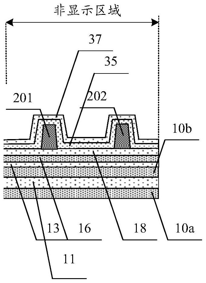
The present application discloses a display substrate, a preparation method, and a display device. The display substrate includes a display area and a non-display area. The non-display area includes a functional layer, a retaining wall arranged on the functional layer, and layer and the encapsulation layer of the retaining wall, the retaining wall includes a bottom surface close to the functional layer, a top surface opposite to the bottom surface, and opposite two sides, at least one side has a recessed structure, and the recessed structure makes the On a plane parallel to the display substrate, the length of the side on the plane is greater than the length of the side on the plane parallel to the display substrate when the side is a plane. In the embodiment of the present application, by adding a recessed structure to the retaining wall and changing the edge shape of the retaining wall, the short-circuit distance between two touch screen panel traces is increased and the risk of short-circuit is reduced.

Description

technical field [0001] The invention relates to the field of display technology, in particular to a display substrate, a preparation method thereof, and a display device. Background technique [0002] In the active matrix organic light emitting diode (Active Matrix Organic Light Emitting Diode, AMOLED) display substrate, the IC (Integrated Circuit, integrated circuit) area has a touch screen wiring horizontal DAM structure, which is prone to short circuit. There are many short-circuit problems in the touch screen traces where the IC crosses the DAM, which affects the overall yield of the screen. Contents of the invention [0003] At least one embodiment of the present invention provides a serial peripheral interface circuit and a display panel to improve display quality. [0004] In order to achieve the purpose of the present invention, at least one embodiment of the present invention provides a display substrate, including a display area and a non-display area, and the n...

Claims


Application Information

Patent Timeline
Patent Type & Authority Patents(China)
IPC IPC(8): H01L27/32H01L51/56
CPCH10K59/88H10K59/40H10K59/00H10K71/00
Inventor 来春荣李世军刘朝
Owner BOE TECH GRP CO LTD
Learn More