a display panel

A display panel and substrate technology, applied in the direction of diodes, semiconductor devices, electrical components, etc., can solve the problem of low transmittance of visible light, achieve the effect of increasing light transmittance and improving camera accuracy

Active Publication Date: 2022-02-22
WUHAN CHINA STAR OPTOELECTRONICS SEMICON DISPLAY TECH CO LTD
View PDF3 Cites 0 Cited by
  • Summary
  • Abstract
  • Description
  • Claims
  • Application Information

AI Technical Summary

Problems solved by technology

[0005] In order to solve the above problems, the present invention provides a display panel, which is used to solve the technical problem that the visible light transmittance of the flexible substrate is low in the prior art, and it is difficult for external visible light to enter the imaging unit when the camera is placed under the panel.

Method used


Image

  • a display panel
  • a display panel
  • a display panel

Examples


Embodiment 1

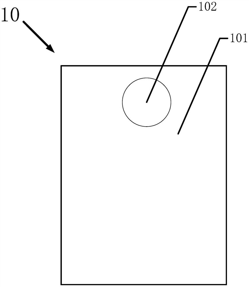
[0037] Such as figure 1 As shown, in this embodiment, the display panel 10 of the present invention includes a display sub-area 101 and an imaging area 102 .

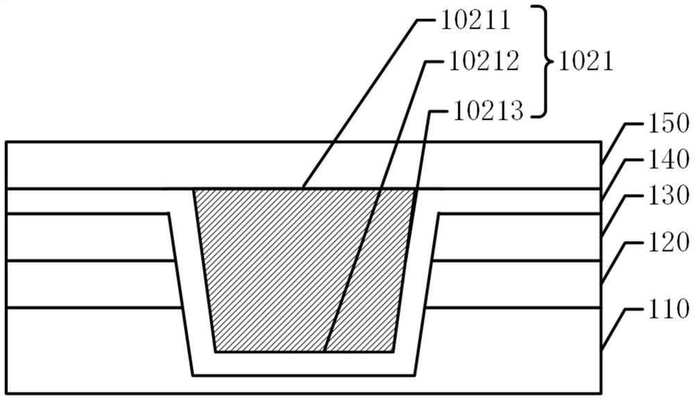
[0038] Such as figure 2 As shown, the display panel 10 further includes a substrate 110 , a thin film transistor layer 120 , an organic light emitting layer 130 , a first barrier layer 140 and a first encapsulation layer 150 .

[0039] The substrate 110 is a flexible substrate, and its material is polyimide material or other similar flexible resin materials or a combination of flexible resin materials and inorganic materials. The substrate 110 is made of light-transmitting materials, so it can accommodate light passing through the substrate 110.

[0040] The thin film transistor layer 120 is disposed on the substrate 110 , and a plurality of circuit structures are disposed on the thin film transistor layer 120 for providing electric energy for displaying by the display panel 10 .

[0041] The organic light-emitting ...

Embodiment 2

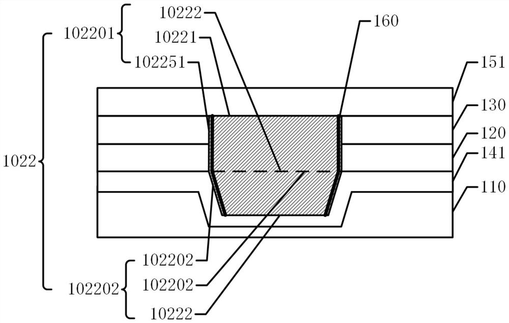
[0047] In this embodiment, the display panel 10 of the present invention includes a display sub-area 101 and an imaging area 102 .

[0048] Such as image 3 As shown, the display panel 10 further includes a substrate 110 , a thin film transistor layer 120 , an organic light emitting layer 130 , a second barrier layer 141 and a second encapsulation layer 151 .

[0049] The substrate 110 is a flexible substrate, and its material is polyimide material or other similar flexible resin materials or a combination of flexible resin materials and inorganic materials. The substrate 110 is made of light-transmitting materials, so it can accommodate light passing through the substrate 110.

[0050] The thin film transistor layer 120 is disposed on the substrate 110 , and a plurality of circuit structures are disposed on the thin film transistor layer 120 for providing electric energy for displaying by the display panel 10 .

[0051] The organic light-emitting layer 130 is disposed on th...


PUM


Abstract

The invention discloses a display panel, which includes an imaging area and a display sub-area surrounding the imaging area, and also includes a substrate; a thin film transistor layer arranged on the substrate; an organic light emitting layer arranged on the thin film transistor layer a groove, provided in the imaging region, the groove penetrates the thin film transistor layer and the organic light-emitting layer and extends to the inside of the substrate. The beneficial effect of the present invention is that the display panel of the present invention has a groove in the imaging area and fills it with a light-transmitting material, which improves the light transmittance of the light and improves the imaging accuracy. The groove adopts a structure with a wide top and a narrow bottom, which is beneficial to The fabrication and subsequent filling of fillers, while the structure with a wide top and a narrow bottom is also conducive to the packaging of the groove.

Description

technical field [0001] The invention relates to the display field, in particular to a display panel. Background technique [0002] At present, the development of display technology is changing with each passing day, and the emergence of various screen technologies provides infinite possibilities for electronic terminals. Especially with the rapid application of display technology represented by OLED (Organic Light Emitting Diode), various mobile terminals with selling points such as "full screen", "special-shaped screen", "under-screen sound" and "under-screen fingerprint" have begun to rapidly develop. promote. [0003] Full screen technology is a relatively broad definition of the display industry for the design of mobile phones with ultra-high screen ratio. The literal explanation is that the front of the mobile phone is all screens, the display interface of the mobile phone is completely covered by the screen, and the four borders of the mobile phone are designed with ...

Claims


Application Information

Patent Timeline
Patent Type & Authority Patents(China)
IPC IPC(8): H01L27/32
CPCH10K59/65H10K59/12
Inventor 张福阳
Owner WUHAN CHINA STAR OPTOELECTRONICS SEMICON DISPLAY TECH CO LTD
Why Eureka
Try Eureka