A stress adjustment layer for semiconductor ultra-thin epitaxial structure

A technology of stress adjustment and epitaxial structure, which is applied in the direction of semiconductor devices, electrical components, nanotechnology, etc., can solve the problems that are not conducive to improving the integration of micro-LED chips, the brightness and resolution cannot be further improved, and the integration cannot be further improved.

Active Publication Date: 2021-08-03
JADE BIRD DISPLAY SHANGHAI LTD
View PDF7 Cites 0 Cited by
  • Summary
  • Abstract
  • Description
  • Claims
  • Application Information

AI Technical Summary

Problems solved by technology

However, in the traditional LED manufacturing process, due to the limitation of the process conditions of photolithography and etching equipment, the etched patterns inevitably present sloped sidewalls.
Due to the appearance of inclined sidewalls, the effective light-emitting area of ​​each LED is smaller than the occupied area of ​​the LED. In order to ensure the effective light-emitting area of ​​the LED, it is impossible to further improve the integration level, which limits the further reduction of the size of the micro-LED chip, which is not conducive to improving The integration level of micro-LED chips makes it impossible to further improve the brightness and resolution of the final product

Method used


Image

  • A stress adjustment layer for semiconductor ultra-thin epitaxial structure
  • A stress adjustment layer for semiconductor ultra-thin epitaxial structure
  • A stress adjustment layer for semiconductor ultra-thin epitaxial structure

Examples


Embodiment Construction

[0024] In order to make the content of the present invention clearer and easier to understand, the content of the present invention will be further described below in conjunction with the accompanying drawings. Of course, the present invention is not limited to this specific embodiment, and general replacements known to those skilled in the art are also covered within the protection scope of the present invention.

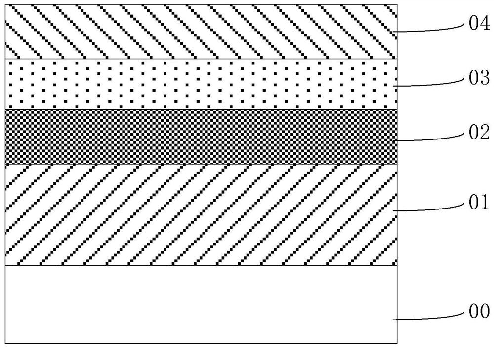
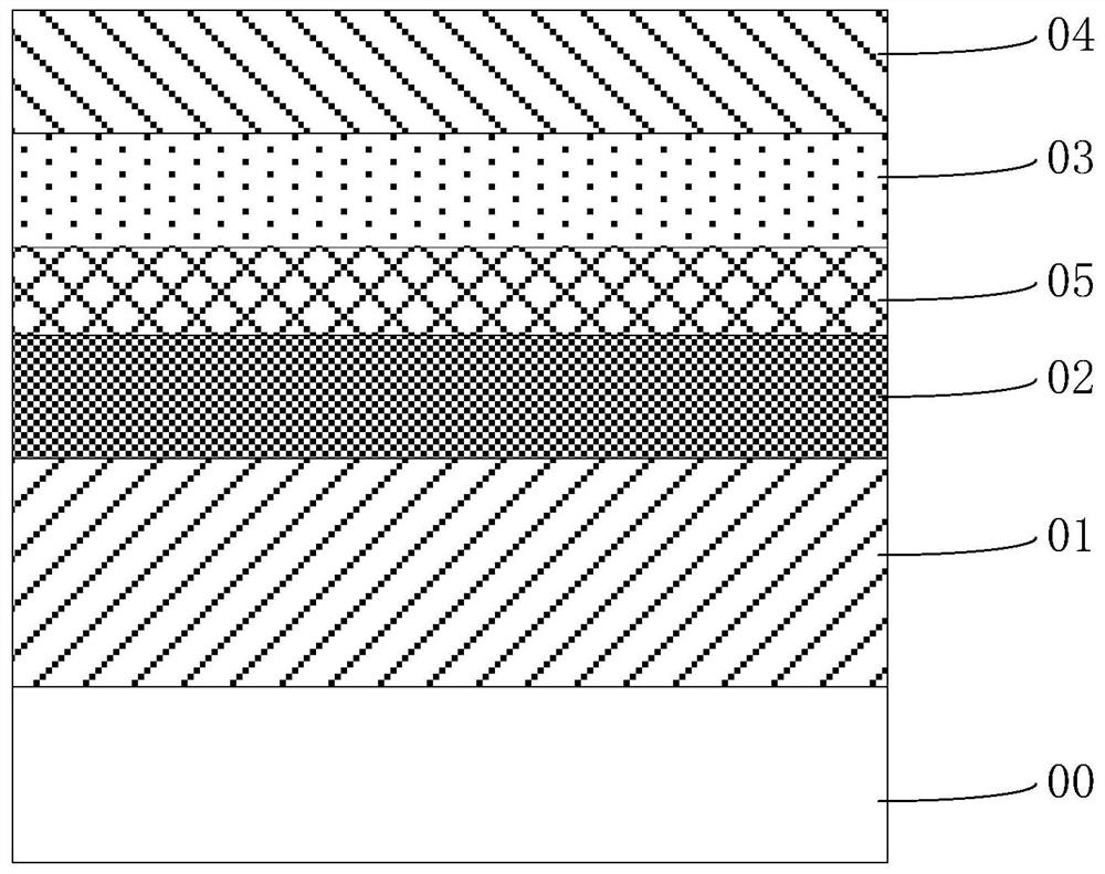
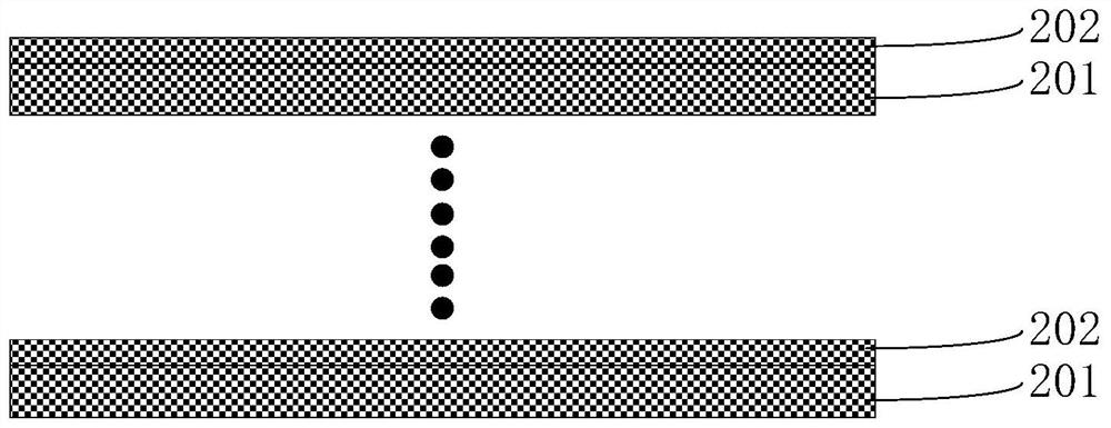
[0025] The stress adjustment layer of the semiconductor ultra-thin epitaxial structure in the present invention includes a multi-layer multi-period stress adjustment layer and a dislocation fine-tuning layer on the top of the multi-layer multi-period stress adjustment layer. It should be noted here that the stress adjustment layer is grown on the epitaxial layer, and the conductivity type of the epitaxial layer is the same as that of the dislocation fine-tuning layer.

[0026] The following is attached Figure 1~4 and Specific Embodiments The present invention wil...


PUM

PropertyMeasurementUnit
thicknessaaaaaaaaaa
thicknessaaaaaaaaaa
thicknessaaaaaaaaaa

Abstract

The invention provides a stress adjustment layer for semiconductor ultra-thin epitaxial structure, which uses a multi-period stress adjustment layer and a first conductivity type dislocation fine-tuning layer on the top of the multi-cycle stress adjustment layer to reduce the stress in the first conductivity type epitaxial layer. stress, and using the first conductivity type dislocation fine-tuning layer to control the dislocation concentration on the surface of the stress-adjusting layer. Since the epitaxial structure is very thin, in the process of fabricating the device, the etching of the epitaxial structure will not cause the sidewall of the epitaxial structure to have a large slope, which is approximately vertical. Since the areas of the top and bottom of the etched epitaxial structure are similar, This overcomes the problem that the top of the traditional epitaxial structure is smaller than the bottom, resulting in a reduction in the effective light-emitting area, improves chip integration, and improves the luminous efficiency per unit area of ​​the device.

Description

technical field [0001] The invention relates to the technical field of an epitaxial structure on a semiconductor substrate, in particular to a stress adjustment layer for a semiconductor ultra-thin epitaxial structure. Background technique [0002] With the advancement of technology and the development of the market, micro-LEDs have gradually become the focus of attention because they are more conducive to the requirements of portable and lightweight products, such as ultra-thin display screens. However, the current technical route of micro-LED is uncertain and the cost is high, which is not conducive to large-scale commercialization. [0003] Furthermore, in the micro-LED chip, the size and spacing of each LED are required to be as small as possible to improve the integration of the chip, so as to effectively ensure the brightness and resolution of the final product. In order to make a small-sized LED, it is necessary to further reduce the size of the LED. However, in the...

Claims


Application Information

Patent Timeline
Patent Type & Authority Patents(China)
IPC IPC(8): H01L33/12B82Y40/00
CPCB82Y40/00H01L33/12
Inventor 游正璋马后永李起鸣
Owner JADE BIRD DISPLAY SHANGHAI LTD
Why Eureka
Try Eureka