Ultra-short-distance micro-lens array interference 3D imaging mobile phone lens

A micro-lens array and lens technology, applied in image communication, telephone structure, television and other directions, can solve the problems of complex and expensive manufacturing of large-diameter optical systems, and achieve the effects of easy placement, improved production efficiency, and short production cycle.

Pending Publication Date: 2019-11-29
乔士琪
View PDF0 Cites 0 Cited by
  • Summary
  • Abstract
  • Description
  • Claims
  • Application Information

AI Technical Summary

Problems solved by technology

Second, it has more advantages in the manufacturing process. The traditional large-aperture optical system is very complicated and expensive to manufacture. The lenses of some well-known telescope systems even use years as a cycle, while the microlens saves a lot of time and only needs a few days. It will be ready in a week

Method used


Image

  • Ultra-short-distance micro-lens array interference 3D imaging mobile phone lens

Examples


Embodiment Construction

[0016] The principles and features of the present invention are described below in conjunction with the accompanying drawings, and the examples given are only used to explain the present invention, and are not intended to limit the scope of the present invention.

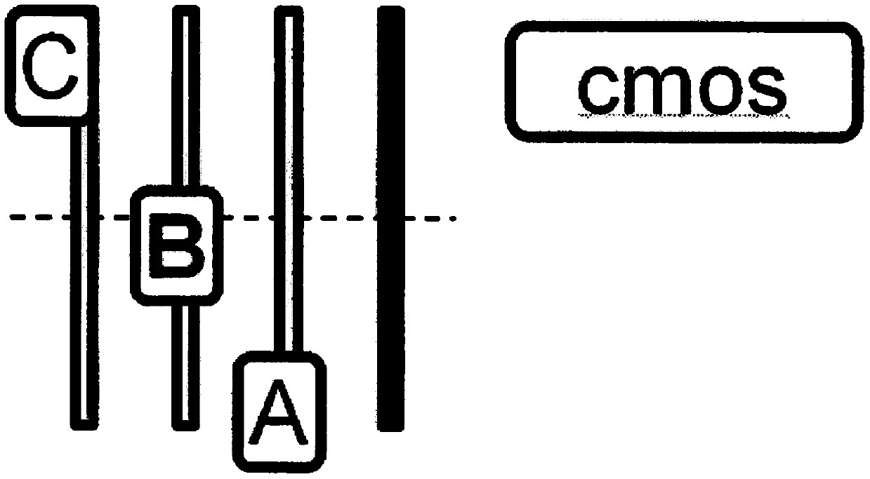
[0017] Such as figure 1 As shown, an ultra-short-distance microlens array interference 3D imaging mobile phone lens includes a CMOS lens and an optical system positioned in front of the CMOS lens. The optical system includes three microlenses arranged in parallel in turn, optical device A, optical Device B, optical device C; the optical device A is close to the CMOS lens, the optical device A, optical device B, optical device C and the CMOS lens have the same size, and the total optical length is 3 mm, and the outer diameter of the lens is less than 6 mm;

[0018] In a specific embodiment, the medium between the CMOS lens and the optical device A is air, and the optical center distance from the CMOS lens to the opti...


PUM

PropertyMeasurementUnit
Focal lengthaaaaaaaaaa

Abstract

The invention relates to an ultra-short-distance micro lens array interference 3D imaging mobile phone lens, which comprises a CMOS lens and an optical system located in front of the CMOS lens, and ischaracterized in that the optical system comprises three micro lenses, an optical device A, an optical device B and an optical device C which are sequentially arranged in parallel. Compared with traditional optical imaging, the technical scheme has the advantages that the volume mass is more advantageous, the mass of the camera can be reduced by 90%, the shape arrangement is more flexible, and compared with a traditional cylinder structure, the camera is easier to arrange; and secondly, the manufacturing process has more advantages, the manufacturing period is short, and the production efficiency can be greatly improved.

Description

technical field [0001] The invention relates to the field of imaging technology devices, in particular to an ultra-short-distance microlens array interference 3D imaging mobile phone lens. Background technique [0002] The traditional optical imaging technology is similar to seeing things with the human eye, through a series of lenses or mirrors, the light from the object side is imaged on the CCD, and then the photoelectric conversion is carried out by the CCD to obtain the image. The microlens interference optical imaging technology is different. It collects light into a photonic integrated circuit through a microlens array, performs imaging in the frequency domain, and then inverse Fourier transforms it to obtain the original image. [0003] This microlens array interference imaging technology is also very impressive in terms of imaging capabilities. For a camera with a height of 500nm, a height of 300km, and a baseline length of 0.5m, the spatial resolution can reach 0.3...

Claims


Application Information

Patent Timeline
IPC IPC(8): H04N5/225H04M1/02H04N13/204
CPCH04M1/0264H04N13/204H04N23/57H04N23/55H04N23/54
Inventor 乔士琪
Owner 乔士琪
Why Eureka
Try Eureka