Semiconductor device testing method and system

A test method and semiconductor technology, which is applied in the direction of single semiconductor device testing, instrumentation, and electrical measurement, can solve the problems of low test accuracy and inability to accurately evaluate the performance of semiconductor devices, and achieve the effect of improving test accuracy

Inactive Publication Date: 2019-12-03
启发(天津)电子科技有限公司
View PDF5 Cites 0 Cited by
  • Summary
  • Abstract
  • Description
  • Claims
  • Application Information

AI Technical Summary

Problems solved by technology

[0003] However, the existing test methods have low test accuracy and cannot accurately evaluate the performance of semiconductor devices

Method used


Image

  • Semiconductor device testing method and system
  • Semiconductor device testing method and system
  • Semiconductor device testing method and system

Examples


Embodiment 1

[0037] This embodiment proposes a semiconductor device testing method, which uses an excitation signal with a frequency less than 1Khz to perform a low-frequency capacitance-voltage test on the semiconductor device to be tested to measure the low-frequency capacitance value; -Voltage test, measured high-frequency capacitance value; use low-frequency capacitance value and high-frequency capacitance value to calculate loss factor curve.

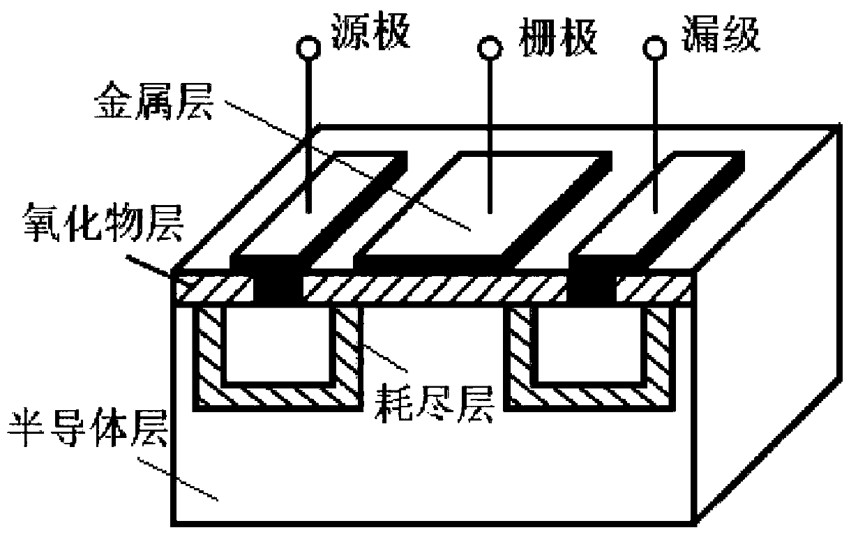
[0038] In this embodiment, the semiconductor device includes a MOS capacitor and a MOS transistor, figure 1 It is a schematic diagram of the structure of the MOS tube in the prior art, refer to figure 1 , The MOS tube includes a MOS structure, and the MOS structure refers to a basic structure composed of a metal layer, an oxide layer, and a semiconductor layer. The capacitance C of the ideal MOS structure is the oxide layer capacitance C ox and space charge capacitance C sc series, that is,

[0039]

[0040] where the oxide layer capacit...

Embodiment 2

[0072] This embodiment proposes a semiconductor device test system, which utilizes the test method in Embodiment 1. The test system includes a control terminal and a tester, and the tester is used to perform low-frequency capacitance-voltage testing of the semiconductor device to be tested by an excitation signal with a frequency less than 1Khz. Test to measure the low-frequency capacitance value; and conduct a high-frequency capacitance-voltage test on the semiconductor device to be tested through an excitation signal with a frequency greater than 1KHz to measure the high-frequency capacitance value; the control terminal is used to use the low-frequency capacitance value and the high-frequency Capacitance values ​​are calculated from the dissipation factor curve.

[0073] In this embodiment, the tester is a high-precision LCR tester, such as Keysight e4980a.

[0074] In this embodiment, preferably, the control terminal includes:

[0075] Calculation module: used to receive t...


PUM


Abstract

The invention provides a semiconductor device testing method and system. When a semiconductor device is tested, low-frequency capacitance-voltage testing is performed on a to-be-tested semiconductor device by an excitation signal with the frequency being smaller than 1Khz, so that a low-frequency capacitance value is measured; high-frequency capacitance-voltage testing is performed on the to-be-tested semiconductor device by an excitation signal with the frequency being larger than 1Khz, so that a high-frequency capacitance value is measured; and a loss factor curve is calculated by using thelow-frequency capacitance value and the high-frequency capacitance value. According to the provided method and system, the capacitance-voltage test is divided into a low-frequency part and a high-frequency part; and the loss factor curve is calculated by using the low-frequency capacitance value and the high-frequency capacitance value obtained by testing. And the low-frequency capacitance-voltagetesting is performed on the to-be-tested semiconductor device by using the excitation signal less than 1Khz, so that the test precision of the loss factor curve is improved.

Description

technical field [0001] Embodiments of the present invention relate to MOS process testing technology, and in particular to a semiconductor device testing method and system. Background technique [0002] Semiconductor parameter testing is a very important part of basic research and applied research in microelectronics, materials, physics, etc. In the exploration of semiconductor device technology, it is often necessary to measure and compare samples obtained from different process processes and process parameters to obtain the best results. Process route and process parameters. Common tests include: C-V (capacitance-voltage) test, I-V (current-voltage) test. [0003] However, the existing test methods have low test accuracy and cannot accurately evaluate the performance of semiconductor devices. Contents of the invention [0004] In order to improve the test accuracy of the loss factor curve when measuring semiconductor devices, the present invention provides a semiconduc...

Claims


Application Information

Patent Timeline
Patent Type & Authority Applications(China)
IPC IPC(8): G01R31/26G01R27/26
CPCG01R27/2694G01R31/2601
Inventor 安博吴海雷刘畅
Owner 启发(天津)电子科技有限公司
Why Eureka
Try Eureka