Process mapping method for FPGA with specific structure

A technology of process mapping and mapping scheme, which is applied in special data processing applications, instruments, calculations, etc., and can solve problems such as unusable and inability to obtain better solutions for mapping objects

Active Publication Date: 2019-12-06
SHENZHEN PANGO MICROSYST CO LTD
View PDF3 Cites 2 Cited by
  • Summary
  • Abstract
  • Description
  • Claims
  • Application Information

AI Technical Summary

Problems solved by technology

[0003] The technical problem to be solved by the present invention is that the traditional process mapping method in the prior art takes the 2-input node netlist as input, and its mapping object can only be the LUT structure, and cannot utilize the LUT5M structure, MUX2L6 structure, and MUX2L7 structure of FPGA devices with unique structures And the problem of MUX2L8 structure resource, this method just can not obtain the better solution that mapping objec...

Method used


Image

  • Process mapping method for FPGA with specific structure
  • Process mapping method for FPGA with specific structure
  • Process mapping method for FPGA with specific structure

Examples


Embodiment Construction

[0052] It should be understood that the specific embodiments described here are only used to explain the present invention, not to limit the present invention.

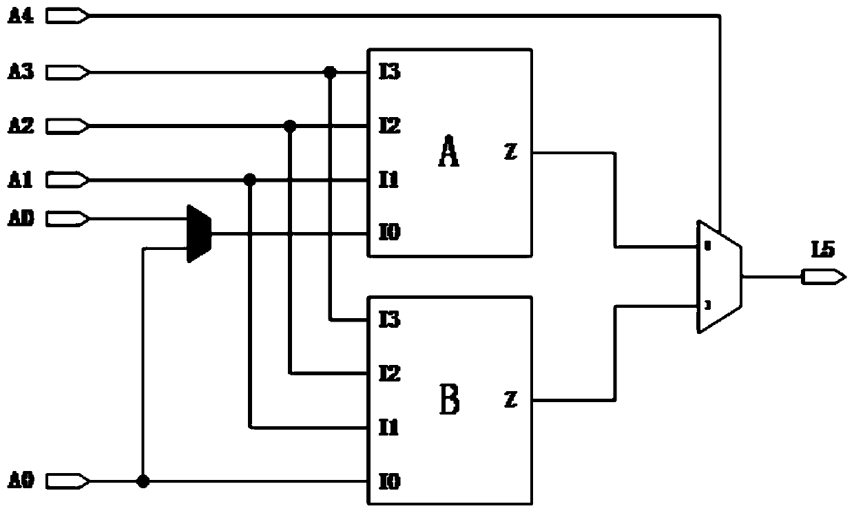
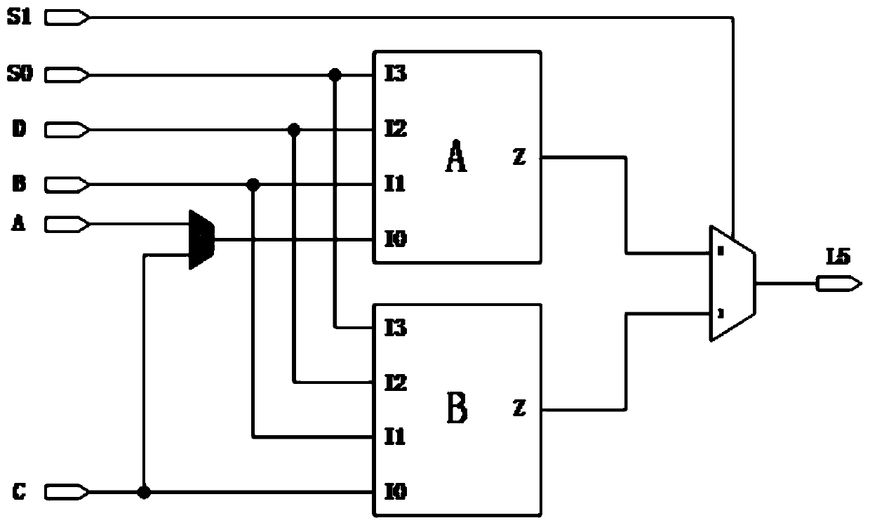
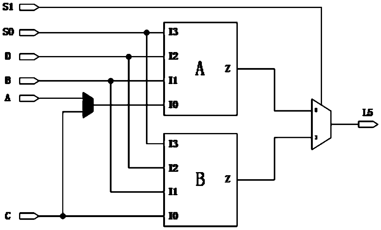
[0053] The FPGA has flexible programmable features, and the programmable features of the combinational logic are mainly realized through a look-up table (LUT, Look Up Table), and the LUT is essentially a RAM (Random Access Memory, random access memory). For example, a LUT with 5 inputs can be regarded as a 32x1 RAM with 5 address lines, which can realize all combinatorial logic within any 5 inputs. Such as Picture 1-1 As shown, the FPGA with a unique structure that the present invention faces has a special LUT structure, and this LUT structure has 6 input terminals, which can realize all combinatorial logics within any 5 inputs, such as Figure 1-2 As shown, the LUT can be configured as a MUX mode—LUT5M to realize the function of MUX4 (4 to 1 multiplexer). Simultaneously the FPGA that the present invention faces al...


PUM


Abstract

The invention provides a process mapping method for an FPGA with a specific structure. An input netlist of the process mapping method comprises at least one two-input first node and at least one MUX2node, and includes the steps: respectively obtaining at least one mapping scheme of which the mapping structure corresponding to the first node is a LUT structure, obtaining at least two mapping schemes that the mapping structure corresponding to the MUX2 node is an LUT structure and the mapping structure corresponding to the MUX2 node is mapped to at least one of an LUT5M structure, an MUX2L6 structure, an MUX2L7 structure and an MUX2L8 structure, and determining the optimal mapping scheme corresponding to the first node and the MUX2 node; and obtaining a map-point node in the first node andthe MUX2 node, and generating a corresponding optimal netlist structure one by one according to the optimal mapping scheme of the first node or the MUX2 node where the map-point node is located. The process mapping method achieves the effects of greatly improving the resource utilization rate of the specific LUT5M mode, the specific MUX2L6 structure, the specific MUX2L7 structure and the specificMUX2L8 structure of the FPGA with the specific structure, reducing the circuit area, reducing the hierarchy of the LUT-level netlist and improving the circuit performance.

Description

technical field [0001] The present invention relates to Field Programmable Gate Array (FPGA, Field Programmable Gate Array) and Electronic Design Automation (EDA, Electronic Design Automation) technical fields, in particular to a technology mapping (Technology Mapping) method for FPGA with a unique structure. Background technique [0002] The traditional process mapping method takes the 2-input node netlist as input, because such a fine-grained netlist is convenient to enumerate as many cuts as possible, so as to obtain better mapping results. But correspondingly, the mapping object can only be the LUT structure, and the LUT5M structure, MUX2L6 structure, MUX2L7 structure and MUX2L8 structure resources of the FPGA device with a unique structure cannot be used. This method cannot obtain the mapping object including LUT5M for circuits rich in MUX nodes. Structure, MUX2L6 structure, MUX2L7 structure and better solution for MUX2L8 structure. Contents of the invention [0003]...

Claims


Application Information

Patent Timeline
IPC IPC(8): G06F17/50
Inventor 郭旭峰
Owner SHENZHEN PANGO MICROSYST CO LTD
Why Eureka
Try Eureka