Semiconductor processing system

A processing system and semiconductor technology, applied in semiconductor/solid-state device manufacturing, electrical components, circuits, etc., can solve problems such as large process equipment space and waste of clean space in workshops

Active Publication Date: 2019-12-10
S Y TECH ENG & CONSTR CO LTD +1
View PDF6 Cites 0 Cited by
  • Summary
  • Abstract
  • Description
  • Claims
  • Application Information

AI Technical Summary

Problems solved by technology

Due to the arrangement of the existing process equipment, the space at the front and rear of the process equipment will be larger, so it will lead to waste of clean space in the workshop

Method used


Image

  • Semiconductor processing system
  • Semiconductor processing system
  • Semiconductor processing system

Examples


Embodiment Construction

[0033] In order to improve the utilization rate of clean space in a semiconductor production plant, an embodiment of the present invention provides a semiconductor processing system. In order to make the purpose, technical solution and advantages of the present invention clearer, the following examples are given to further describe the present invention in detail.

[0034] When the present application mentions ordinal numerals such as "first", "second", "third" or "fourth", unless it really expresses the meaning of order according to the context, it should be understood as only for distinction.

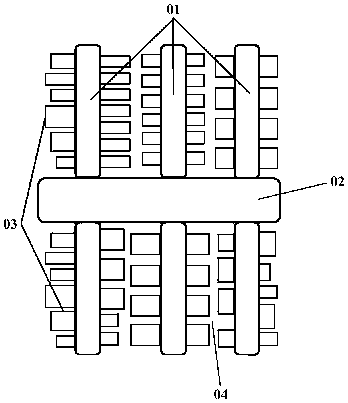
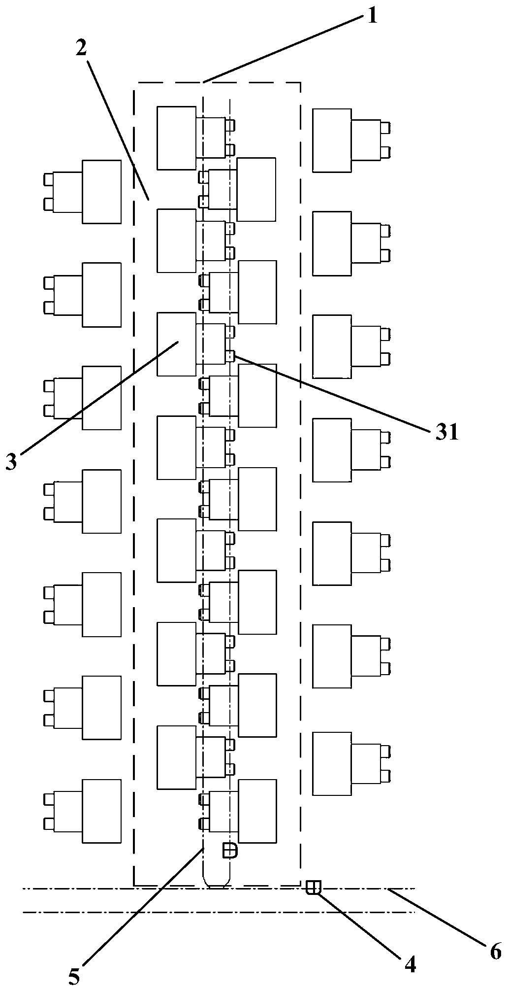
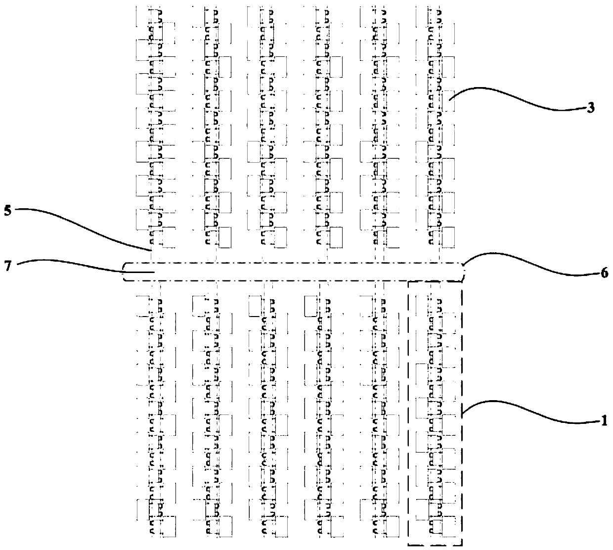
[0035] Such as Figure 2 to Figure 3 As shown, the embodiment of the present invention provides a semiconductor processing system, including: a plurality of semiconductor processing groups 1, an operation channel 2 is provided between two adjacent semiconductor processing groups 1, and the semiconductor processing group 1 includes a handling device 4, The moving track 5 of the handli...


PUM


Abstract

The invention discloses a semiconductor processing system to improve the utilization rate of a clean space in a semiconductor production workshop. The semiconductor processing system comprises a plurality of semiconductor processing groups, and an operation channel is arranged between every two adjacent semiconductor processing groups. Each semiconductor processing group comprises a carrying device, a carrying device movement track and two rows of process equipment. The process equipment comprises loading interfaces. For each semiconductor processing group, the two rows of process equipment are oppositely arranged in a staggered manner, the orientations of the loading interfaces are opposite, the carrying device movement track is arranged above the process equipment, and the carrying device can move along the carrying device movement track and convey carried electronic device products to the corresponding loading interfaces.

Description

technical field [0001] The invention relates to the technical field of semiconductor processing, in particular to a semiconductor processing system. Background technique [0002] The semiconductor production line basically adopts a harbor-style equipment arrangement similar to a fishbone. Refer to figure 1 , the harbors 01 are connected through the central transport corridor 02, and the automated material handling system is responsible for transporting the carriers filled with wafers between the harbors 01 and inside the harbor 01. [0003] refer to figure 1 As shown, when the Overhead Hoist Transport (OHT, Overhead Hoist Transport) is used inside Harbor 01 to transport the carrier containing wafers to the loading interface of process equipment 03, the loading interface of process equipment 03 should be located at the front of the track of the overhead transport trolley. Below, multiple process equipment 03 should be arranged side by side so that the handling system can pr...

Claims


Application Information

Patent Timeline
Patent Type & Authority Applications(China)
IPC IPC(8): H01L21/67
CPCH01L21/67173
Inventor 李强李卫安利壮
Owner S Y TECH ENG & CONSTR CO LTD
Why Eureka
Try Eureka