Silicon wafer cutting method and device

A cutting method and cutting device technology, applied in welding/welding/cutting items, laser welding equipment, manufacturing tools, etc., can solve problems such as trajectory deviation and poor quality, and achieve the effect of avoiding damage

Pending Publication Date: 2019-12-13
DATONG XINCHENG NEW MATERIAL CO LTD
View PDF9 Cites 0 Cited by
  • Summary
  • Abstract
  • Description
  • Claims
  • Application Information

AI Technical Summary

Problems solved by technology

[0003] In order to overcome the problems existing in the related technologies, the present invention provides a silicon wafer cutting method and a cutting device, which can solve the problems of poor quality of the two edge positions of cutting in and cutting out and track deviation during asymmetric cutting in the current thermal splitting method

Method used


Image

  • Silicon wafer cutting method and device
  • Silicon wafer cutting method and device

Examples


Embodiment Construction

[0022] In order to enable those skilled in the art to better understand the technical solutions in the present invention, the technical solutions in the embodiments of the present invention will be clearly and completely described below in conjunction with the drawings in the embodiments of the present invention. Obviously, the described The embodiments are only some of the embodiments of the present invention, not all of them. Based on the embodiments of the present invention, all other embodiments obtained by persons of ordinary skill in the art without making creative efforts shall fall within the protection scope of the present invention.

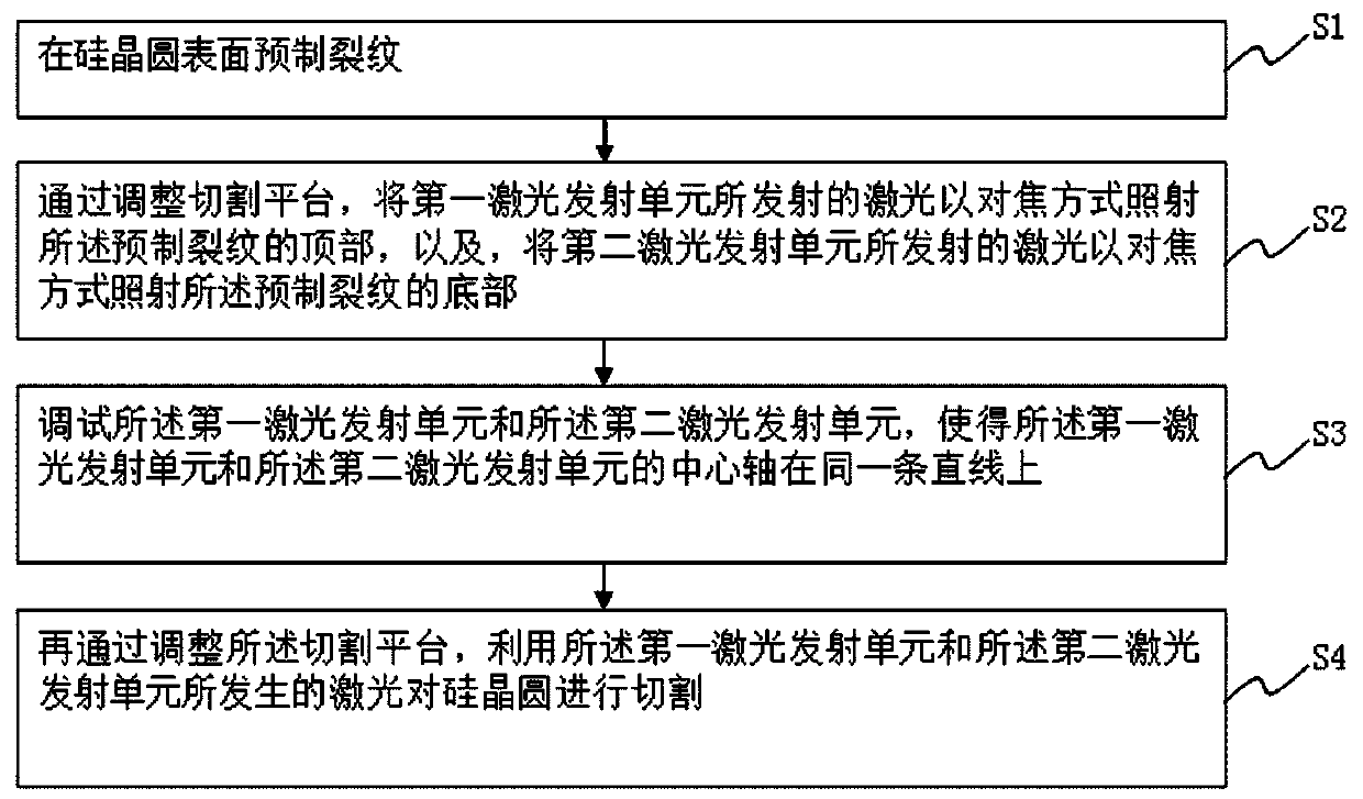
[0023] A first aspect of the present disclosure provides a silicon wafer dicing method, the dicing method comprising the following steps:

[0024] S1: prefabricating cracks on the surface of the silicon wafer;

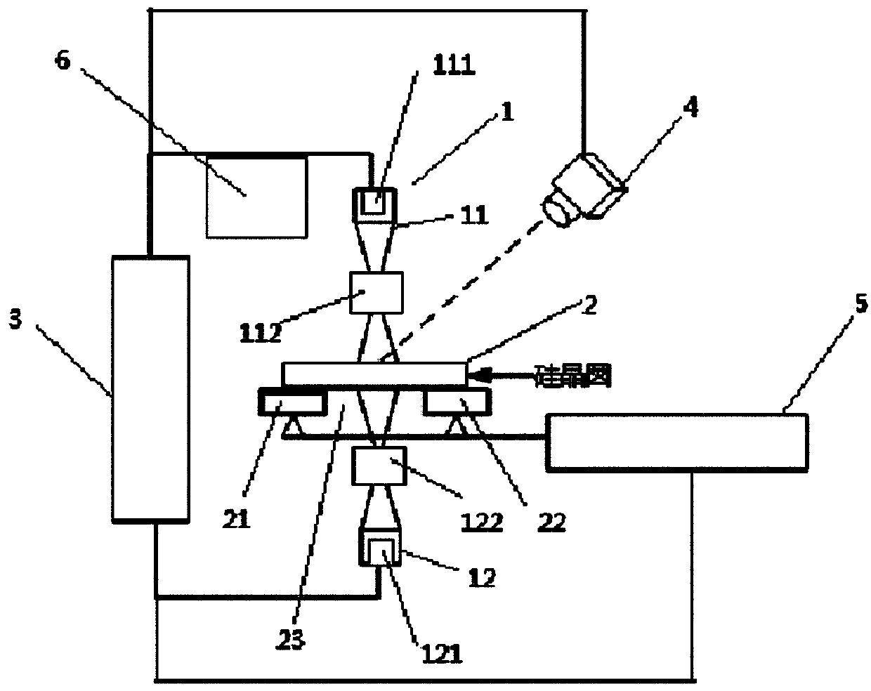
[0025] S2: By adjusting the cutting platform, irradiate the laser emitted by the first laser emitting unit on the top of the ...


PUM


Abstract

The invention discloses a silicon wafer cutting method and device. The silicon wafer cutting method comprises the following steps: firstly, prefabricating cracks on the surface of a silicon wafer; byadjusting a cutting platform, irradiating the top of the precast cracks by laser emitted by a first laser emitting unit in a focusing manner, and irradiating the bottom of the precast cracks by the laser emitted by a second laser emitting unit in a focusing manner; debugging the first laser emitting unit and the second laser emitting unit so that the central axes of the first laser emitting unit and the second laser emitting unit are on the same straight line; and then adjusting the cutting platform, and using the laser generated by the first laser emitting unit and the second laser emitting unit to cut the silicon wafer. The silicon wafer cutting method and device can obviously solve the problems that poor quality of cut-in and cut-out edge positions and track deviation during asymmetriccutting occur by using a conventional hot cracking method.

Description

technical field [0001] The invention relates to the technical field of chip manufacturing, in particular to a silicon wafer cutting method and a cutting device. Background technique [0002] Silicon wafers are widely used in the manufacture of semiconductor devices. Silicon wafer dicing is a key process in the packaging process. The traditional ultra-thin diamond grinding wheel cutting method has low processing efficiency, and the finished product is prone to chipping. Laser cutting technology belongs to non-contact cutting. Laser cutting can solve the problem of edge chipping in mechanical cutting, and there is no problem of tool wear. From the cutting mechanism, laser cutting technology can be divided into two modes, one is the way of removing material, such as laser melting / vaporization cutting, water guided laser cutting, etc.; the other is the way of no material removal, that is, laser thermal cutting Crack cutting (also known as laser thermal stress cutting, laser con...

Claims


Application Information

Patent Timeline
IPC IPC(8): B23K26/38
CPCB23K26/38B23K2103/56
Inventor 柴万红
Owner DATONG XINCHENG NEW MATERIAL CO LTD
Why Eureka
Try Eureka