HDI printed circuit board manufacturing method and HDI printed circuit board

A printed circuit board and manufacturing method technology, applied in printed circuit manufacturing, printed circuits, printed circuit components and other directions, can solve problems such as poor layered foaming, reduce manufacturing cycles, increase wiring area, and improve manufacturing yields Effect

Inactive Publication Date: 2019-12-13
深圳明阳电路科技股份有限公司
View PDF2 Cites 5 Cited by
  • Summary
  • Abstract
  • Description
  • Claims
  • Application Information

AI Technical Summary

Problems solved by technology

For this reason, an object of the embodiment of the present invention is to provide a method for manufacturing an HDI printed circuit board and an HDI printed circuit board made by the method, which can solve the phenomenon of poor delamination and foaming in the existing manufacturing process

Method used


Image

  • HDI printed circuit board manufacturing method and HDI printed circuit board
  • HDI printed circuit board manufacturing method and HDI printed circuit board
  • HDI printed circuit board manufacturing method and HDI printed circuit board

Examples


Embodiment 1

[0036] Embodiment 1 provides a kind of manufacturing method of HDI printed circuit board, and this method comprises the following steps:

[0037] S1: core board pretreatment step;

[0038] S2: Pressing and graphic transfer steps; intermediate processing steps are included between the pressing and graphic transfer steps;

[0039] S3: graphic electroplating step;

[0040] S4: post-processing step.

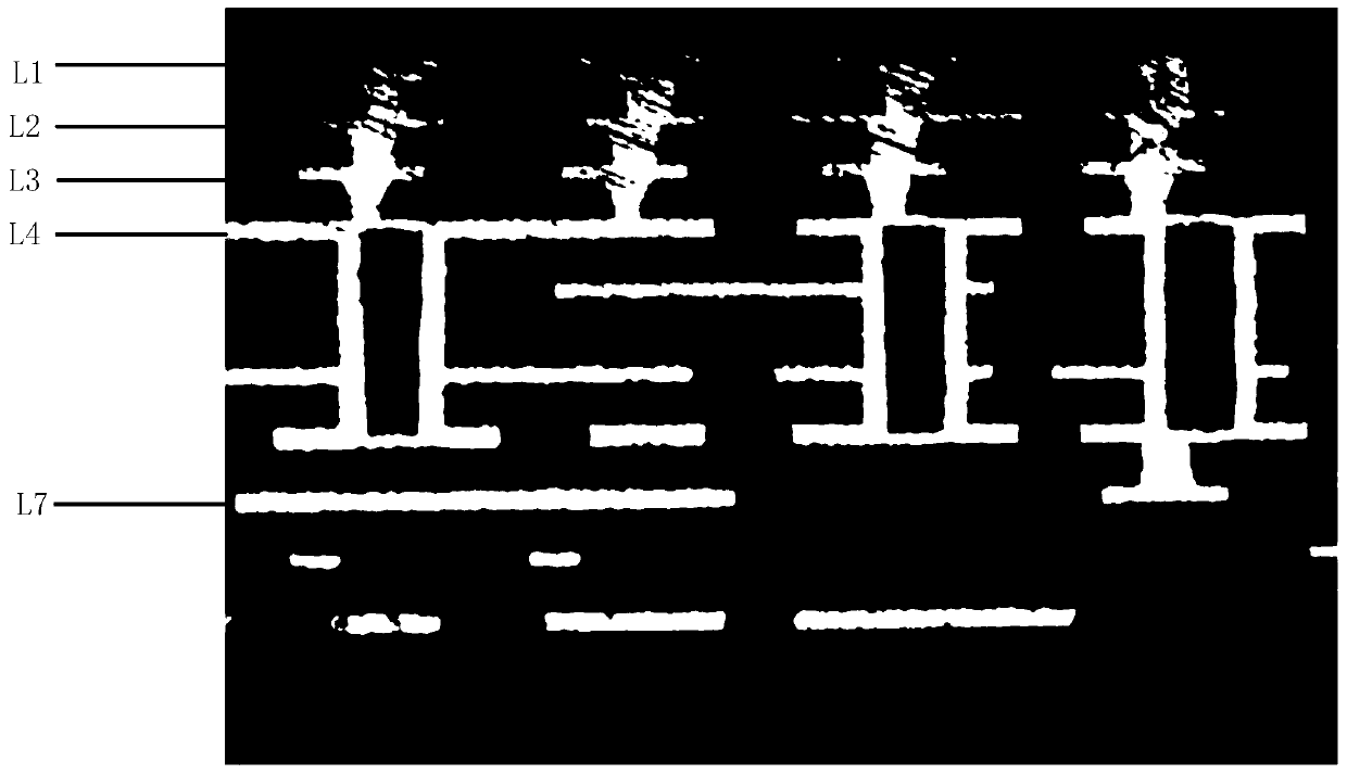
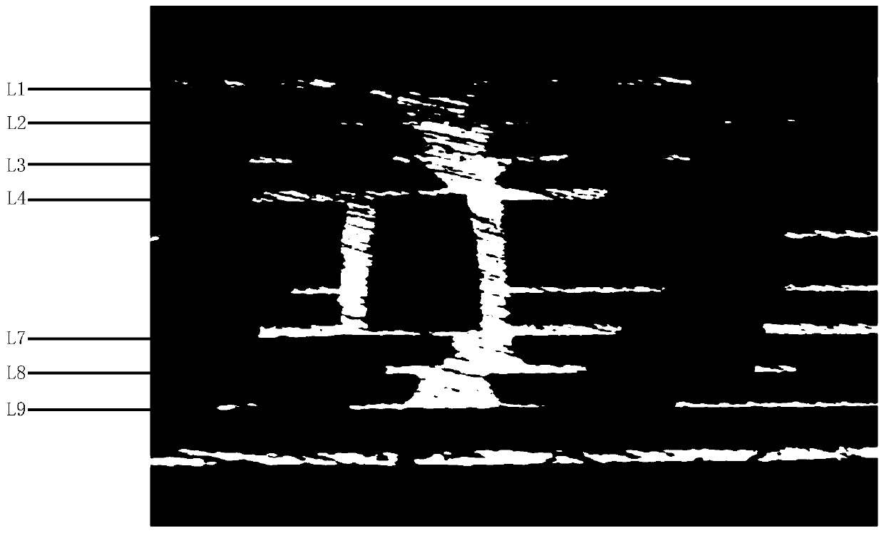
[0041] In step S1, the core board pretreatment step includes material cutting and inner-layer circuit fabrication, and the inner-layer circuit fabrication is to fabricate L5 and L6 layer circuits.

[0042] Step S2 actually includes all the intermediate processing steps between each pressing step and graphic transfer step and the corresponding pressing step and graphic transfer step;

[0043] The pressing steps include the first pressing step, the second pressing step, the third pressing step and the fourth pressing step; the pattern transfer step includes the first graphic transfe...

Embodiment 2

[0077] Embodiment 2 is provided based on Embodiment 1, and its difference is:

[0078] In step S211, the copper of the circuit board after the pressing step is reduced to a copper thickness of 9 μm;

[0079] In step S214, the resin plug hole is to fill the hole with non-insulating resin, so that the hole becomes a whole, which can increase the wiring and increase the function design of the hole; the plug hole adopts a special plug resin printing machine equipment Production, plugging speed: 200mm / min; front ink pressure: 1.8bar, rear ink pressure: 4.0bar, baking before plugging, among which baking plate parameters: 100°C / 40min, baking plate parameters after plugging: 110°C / 40min, after the hole is plugged, the protruding resin is smoothed with a grinding machine.

Embodiment 3

[0081] Embodiment 3 is provided based on Embodiment 1, and its difference is:

[0082] In step S211, the copper of the circuit board after the pressing step is reduced to a copper thickness of 10 μm;

[0083] In step S214, the resin plug hole is to fill the hole with non-insulating resin, so that the hole becomes a whole, which can increase the wiring and increase the function design of the hole; the plug hole adopts a special plug resin printing machine equipment Production, plugging speed: 200mm / min; front ink pressure: 1.8bar, rear ink pressure: 4.0bar, baking before plugging, among which the baking plate parameter: 100℃ / 40min, the baking plate parameter after plugging: 150℃ / 60min, after the hole is plugged, the protruding resin is smoothed with a grinding machine.


PUM


Abstract

The invention provides an HDI printed circuit board manufacturing method and an HDI printed circuit board. The HDI printed circuit board manufacturing method comprises the steps of core board pretreatment, pressing and pattern transfer, pattern plating and post process. According to the invention, a blind hole and a mechanical buried hole are combined through four lamination steps; the wiring areais maximized; the problems of delamination and poor blistering in the existing manufacturing process are solved; a copper reduction process is added after each lamination step; all holes are plated through spot plating, which ensures that the copper thickness of an etched circuit does not exceed 12 microns; and the method improves the production yield, reduces the production cycle, and reduces the cost.

Description

technical field [0001] The invention relates to the field of manufacturing printed circuit boards, in particular to a method for manufacturing an HDI printed circuit board and the HDI printed circuit board. Background technique [0002] With the increasing demand of the world's electronic consumer goods market and the development of electronic technology, the functions of electronic products are becoming more and more complex, the performance is getting better and better, the volume is getting smaller and lighter, and the weight of printed boards is getting lighter. The requirements are getting higher and higher, especially in the wide application of HDI boards. [0003] HDI (High Density Interconnector) technology is a technology for producing printed circuit boards. It uses a circuit board with a relatively high density of circuit distribution using micro-blind buried hole technology. The wiring of this technology on the circuit board Distributed and multi-level interconn...

Claims


Application Information

Patent Timeline
Patent Type & Authority Applications(China)
IPC IPC(8): H05K3/46H05K1/02
CPCH05K1/0298H05K3/4644
Inventor 孙启双张彦芬
Owner 深圳明阳电路科技股份有限公司
Why Eureka
Try Eureka