Method for manufacturing large-size low-defect silicon carbide single crystal

A silicon carbide single crystal and manufacturing method technology, applied in chemical instruments and methods, single crystal growth, single crystal growth, etc., can solve problems such as large pressure control range, difficult growth speed, and aggravated dislocation increase rate, so as to avoid Effects of secondary damage, cost reduction, and avoidance of seed crystal ablation

Active Publication Date: 2019-12-17
BEIJING TIANKE HEDA SEMICON CO LTD +3
View PDF8 Cites 10 Cited by
  • Summary
  • Abstract
  • Description
  • Claims
  • Application Information

AI Technical Summary

Problems solved by technology

Since the temperature of this secondary process is still above the growth temperature, the control range of the pressure is very large, and it is difficult to control the growth rate
Moreover, if the pressure is too low, the growth rat

Method used


Image

  • Method for manufacturing large-size low-defect silicon carbide single crystal
  • Method for manufacturing large-size low-defect silicon carbide single crystal
  • Method for manufacturing large-size low-defect silicon carbide single crystal

Examples


Embodiment 1

[0052] After charging the furnace according to the normal sublimation recrystallization method, under the vacuum state, when the temperature reaches 1580°C, feed SiH at a flow rate of 50 mL / min into the crucible through the graphite pipeline. 4 The gas stays at this temperature for 20 minutes;

[0053] Subsequently, the vacuum was stopped, Ar gas was introduced into the furnace body, the pressure was controlled at 5Kpa, and the C 3 h 8 Gas, perform low-speed homoepitaxial growth, and keep it for 10 hours;

[0054] Then, fill the Ar gas quickly to 30,000 Pa and stop filling the C 3 h 8 . After that, raise the temperature to 2200°C and lower the Ar gas pressure to 2000Pa to carry out normal SiC single crystal growth.

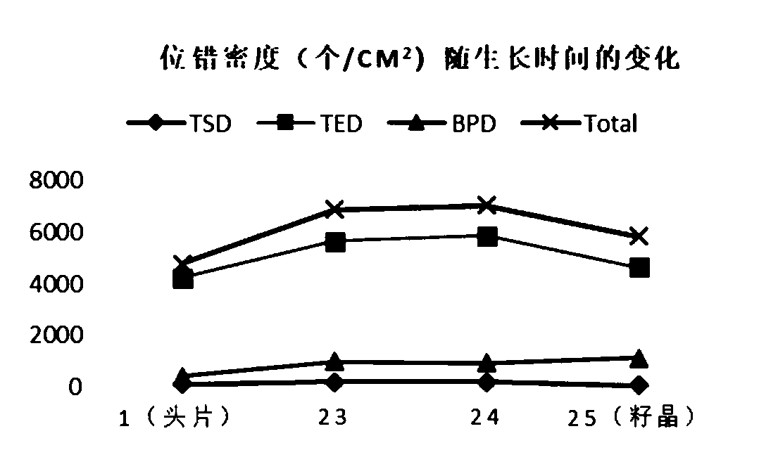
[0055] For silicon carbide single crystal ingots grown by this process, the dislocation density of the initial extended wafer is 1.1 times that of the seed crystal, and the dislocation density of the wafer at the end of growth is 5200 / cm 2 . The SiC single ...

Embodiment 2

[0057] After charging the furnace according to the normal sublimation recrystallization method, under the vacuum state, when the temperature reaches 1640°C, stay at this temperature for 15 minutes;

[0058] Subsequently, the vacuum was stopped, Ar gas was introduced into the furnace body, the pressure was controlled at 4KPa, and the C 3 h 8 Gas, perform low-speed homoepitaxial growth, and keep it for 8 h;

[0059] Then, fill the Ar gas quickly to 30,000 Pa and stop filling the C 3 h 8 . Afterwards, the temperature was raised to 2200° C., and the Ar gas pressure was lowered to 2000 Pa to perform normal SiC single crystal growth.

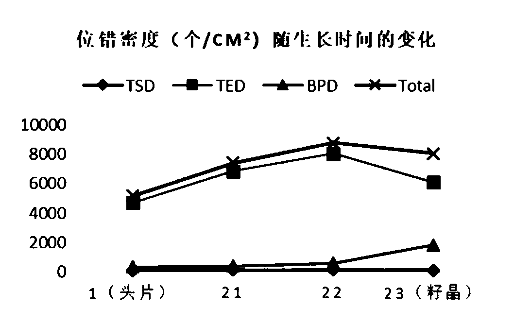
[0060] For silicon carbide single crystal ingots grown by this process, the dislocation density of the extended wafer at the initial stage is 1.2 times the dislocation density of the seed crystal, and the dislocation density of the wafer at the end of growth is 4800 pieces / cm 2 . The SiC single crystal ingot grown with this embodiment changes wi...


PUM


Abstract

In order to solve the problem that dislocation and other defects are greatly increased during seed crystal growth, the invention provides a SiC single crystal growth method capable of obviously reducing the dislocation density from the initial growth stage, thereby manufacturing SiC single crystals with lower dislocation density from the initial growth stage to the final growth stage. The invention relates to a manufacturing method of a silicon carbide single crystal block. According to the manufacturing method of the silicon carbide single crystal block, the silicon carbide single crystal block is prepared by growing the silicon carbide single crystals by using a sublimation recrystallization method on the growth surface of seed crystals generated by the silicon carbide single crystals, in the initial growth stage of the silicon carbide single crystals, a temperature range of 1200 DEG C to 2000 DEG C is adopted, and maintained for more than 10 minutes, then, the pressure is controlledto be between 100 Pa and 10 Kpa; and the pressure of a furnace body is kept constant, a certain flow of hydrocarbon gas is introduced into a growth furnace to enable the surface of the seed crystalsto grow homogeneously at a speed of less than 50 mu/h, and after growing for a period of time, the temperature and the pressure are adjusted to conventional growth conditions at a certain speed to obtain a SiC single crystal ingot with a target thickness.

Description

technical field [0001] The invention relates to a method for manufacturing a silicon carbide single crystal with low dislocation density and high crystal quality. The silicon carbide single crystal wafer prepared by the manufacturing method of the present invention is mainly used as various semiconductor electronic devices or their substrates. In particular, the present invention relates to silicon carbide single crystal wafers cut out from bulk silicon carbide single crystals grown by sublimation recrystallization, wafers cut out from the initial stage of growth of bulk silicon carbide single crystals, and The error density did not increase significantly. Background technique [0002] Silicon carbide (SiC) is an emerging third-generation semiconductor material. Compared with the first-generation silicon and the second-generation gallium arsenide, it has a breakdown field strength 10 times that of silicon, 5 times that of gallium arsenide, and 3 times that of gallium arseni...

Claims


Application Information

Patent Timeline
IPC IPC(8): C30B29/36C30B23/02
CPCC30B23/002C30B23/005C30B23/025C30B29/36
Inventor 娄艳芳刘春俊彭同华王波赵宁杨建
Owner BEIJING TIANKE HEDA SEMICON CO LTD
Why Eureka
Try Eureka