Semiconductor device and formation method thereof

A semiconductor and device technology, applied in the field of semiconductor devices and their formation, can solve problems such as poor performance of semiconductor devices, and achieve the effect of improving performance and avoiding damage

Active Publication Date: 2019-12-17
SEMICON MFG INT (SHANGHAI) CORP +1
View PDF6 Cites 0 Cited by
  • Summary
  • Abstract
  • Description
  • Claims
  • Application Information

AI Technical Summary

Problems solved by technology

[0004] However, the performance of semiconductor devices composed of MOS transistors formed in the prior art is poor

Method used


Image

  • Semiconductor device and formation method thereof
  • Semiconductor device and formation method thereof
  • Semiconductor device and formation method thereof

Examples


Embodiment Construction

[0034] As mentioned in the background, semiconductor devices formed in the prior art have poor performance.

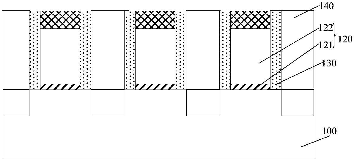
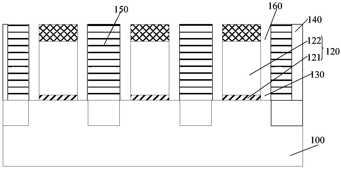
[0035] Figure 1 to Figure 2 It is a structural schematic diagram of the formation process of a semiconductor device.

[0036] refer to figure 1 , providing the substrate 100; forming a gate structure 120, a spacer 130 and a dielectric layer 140, the gate structure 120 is located on the substrate 100, the spacer 130 is located on the sidewall of the gate structure 120, and the dielectric layer 140 is located on the substrate 100 around the gate structure 120 and the spacer 130 .

[0037] The gate structure 120 includes a gate dielectric layer 121 on the surface of the substrate 100 and a gate electrode layer 122 on the gate dielectric layer 121 .

[0038] refer to figure 2 , Form plugs 150 in the dielectric layer 140 on both sides of the gate structure 120 and spacer 130; after forming the plug 150, etch and remove the spacer 130 (refer to figure 1 ), a gap 160 ...


PUM


Abstract

The invention discloses a semiconductor device and a formation method thereof. The method comprises the steps of forming a gate structure, a first side wall, a second side wall and a first dielectriclayer, wherein the gate structure is positioned on a substrate, the gate structure comprises a gate dielectric layer positioned on the surface of the substrate, the side wall of the gate structure comprises a first side wall region and a second side wall region positioned on the first side wall region, the first side wall is positioned on the surface of the first side wall region and covers the side wall of the gate dielectric layer, the second side wall is positioned on the surface of the second side wall region and is positioned on the top surface of the first side wall, the first side walland the second side wall are made of different materials, and the first dielectric layer is positioned on the substrate around the gate structure, the first side wall and the second side wall; formingplugs in the first dielectric layer on two sides of the gate structure, the first side wall and the second side wall respectively; and then, etching to remove the second side wall, forming a gap on the first side wall, wherein the gap is positioned between the second side wall region of the gate structure and the plug. The performance of the semiconductor device is improved according to the method.

Description

technical field [0001] The invention relates to the field of semiconductor manufacturing, in particular to a semiconductor device and a forming method thereof. Background technique [0002] MOS transistors are one of the most important components in modern integrated circuits. The basic structure of a MOS transistor includes: a semiconductor substrate; a gate structure located on the surface of the semiconductor substrate; a source region located in the semiconductor substrate on one side of the gate structure; and a drain region located in the semiconductor substrate on the other side of the gate structure. [0003] The working principle of the MOS transistor is: by applying a voltage to the gate structure, the current in the channel at the bottom of the gate structure is adjusted to generate a switching signal. [0004] However, the performance of semiconductor devices formed by MOS transistors formed in the prior art is relatively poor. Contents of the invention [00...

Claims


Application Information

Patent Timeline
Patent Type & Authority Applications(China)
IPC IPC(8): H01L21/8234H01L27/088
CPCH01L21/823431H01L21/823468H01L27/088H01L27/0886H01L29/66545H01L29/4991H01L29/6653H01L29/66575H01L29/41791H01L29/66795H01L29/7851H01L21/76897H01L21/7682H01L21/823437H01L21/0332H01L21/76829H01L21/0337
Inventor 唐粕人
Owner SEMICON MFG INT (SHANGHAI) CORP
Why Eureka
Try Eureka