Carbon nanotube field effect transistor sensor and manufacturing method thereof

A field-effect transistor and carbon nanotube technology, which is applied in the field of carbon nanotube field-effect transistor sensor and its preparation, can solve the problem of low sensitivity, difficulty in directly modifying the surface of carbon nanotube layer, and good products of carbon nanotube field-effect transistor sensor Low efficiency and other problems, to achieve the effect of improving sensitivity and improving sensing efficiency

Inactive Publication Date: 2019-12-20
PEKING UNIV +2
View PDF7 Cites 3 Cited by
  • Summary
  • Abstract
  • Description
  • Claims
  • Application Information

AI Technical Summary

Problems solved by technology

[0005] In order to solve the above-mentioned technical problems, the application provides a carbon nanotube field effect transistor type sensor and its preparation method, to solve the difficulty in direct modification of the surface of the carbon nanotube layer in the prior art, resulting in the carbon nanotube field effect transistor The problem of low yield and low sensitivity of type sensor

Method used


Image

  • Carbon nanotube field effect transistor sensor and manufacturing method thereof
  • Carbon nanotube field effect transistor sensor and manufacturing method thereof
  • Carbon nanotube field effect transistor sensor and manufacturing method thereof

Examples


Embodiment Construction

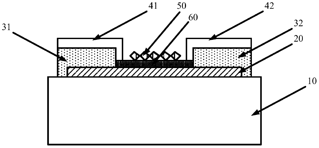
[0050] As mentioned in the background art, carbon nanotubes have a size of 1-2 nm and are easily regulated by external molecules, so they are very suitable for use as biosensors. However, in the prior art, it is very difficult to directly modify the surface of the sensitive layer of the carbon nanotube field effect transistor sensor on the carbon nanotube layer, because the carbon nanotubes in the carbon nanotube layer are formed by carbon atoms hybridized with SP2 The tubular structure of the substance has only in-plane delocalized large π bonds on the surface, and the surface lacks out-of-plane dangling bonds, and the sensitive layer cannot be stably formed on the carbon nanotube layer in a covalently modified manner through dangling bonds.

[0051] Some studies have produced defects by destroying carbon nanotubes to generate dangling bonds, so that the sensitive layer can be covalently modified through the dangling bonds, or the sensitive layer can be realized by ππ bond sta...


PUM


Abstract

The invention discloses a carbon nanotube field effect transistor sensor and a manufacturing method thereof. The carbon nanotube field effect transistor sensor is characterized in that one side, deviating from a substrate, of a carbon nanotube layer is provided with an ultrathin dielectric layer capable of uniformly covering the carbon nanotube layer. When a sensitive layer adsorbs a target substance in the working process, the electrochemical performance generated by the carbon nanotube layer as a channel can be effectively regulated and controlled, so that the effect of the sensitive layer on the channel is more comprehensive and average; the sensing efficiency of the carbon nanotube field effect transistor sensor is improved effectively; and the sensitivity of the carbon nanotube fieldeffect transistor sensor is enhanced. In the presence of the dielectric layer, a dangling bond which can be connected with a covalent bond is provided for the modification of the sensitive layer, so that the sensitive layer can be arranged on the dielectric layer in a covalent modification way; the modification method for the sensitive layer is extended; and the problem of low yield of the conventional carbon nanotube field effect transistor sensor is solved.

Description

technical field [0001] The present application relates to the field of semiconductor technology, more specifically, to a carbon nanotube field effect transistor sensor and a preparation method thereof. Background technique [0002] Carbon nanotube field effect transistor type sensors can be used as gas sensors to detect specific gas molecules in gases, or as biosensors to detect specific biological substances in samples. [0003] The detection principle of the carbon nanotube field effect transistor type sensor is basically: the sensitive layer after capturing the target substance will change the channel conductance of the carbon nanotubes near it, and then change the electrical output parameters of the carbon nanotube field effect transistor. Detectors can determine whether there is a target substance in the sample by whether the electrical output parameters change, or even determine the concentration of the target substance in the sample by the magnitude of the change in t...

Claims


Application Information

Patent Timeline
IPC IPC(8): G01N27/414H01L29/06H01L29/16H01L21/336H01L29/78
CPCG01N27/414G01N27/4146H01L29/0665H01L29/16H01L29/66477H01L29/78
Inventor 肖梦梦张志勇彭练矛
Owner PEKING UNIV
Why Eureka
Try Eureka