PCB automatic wiring system and method

An automatic wiring and wiring technology, applied in special data processing applications, instruments, electrical digital data processing, etc., can solve the problems of low wiring efficiency and poor wiring effect

Active Publication Date: 2019-12-24
INST OF SOFTWARE - CHINESE ACAD OF SCI
View PDF12 Cites 13 Cited by
  • Summary
  • Abstract
  • Description
  • Claims
  • Application Information

AI Technical Summary

Problems solved by technology

[0004] The purpose of this application is to provide a PCB automatic wiring system and method to alleviate the technical problems of low wiring efficiency and poor wiring effect in the prior art

Method used


Image

  • PCB automatic wiring system and method
  • PCB automatic wiring system and method
  • PCB automatic wiring system and method

Examples


Embodiment Construction

[0052] The technical solutions of the present application will be clearly and completely described below in conjunction with the embodiments. Apparently, the described embodiments are part of the embodiments of the present application, not all of them. Based on the embodiments in this application, all other embodiments obtained by persons of ordinary skill in the art without making creative efforts belong to the scope of protection of this application.

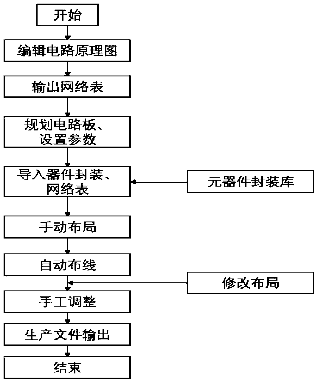
[0053] Wiring is a key step in PCB design, and its function is to connect components through wires to achieve specific functions. In PCB design, it is often desirable to use automatic routing to improve efficiency and save time. figure 1 It is the process of traditional PCB design.

[0054] The traditional PCB design process takes a lot of time in the process of schematic design, PCB layout, etc. After the automatic wiring process, it needs to be adjusted manually according to the needs. The whole process is not highly automa...


PUM


Abstract

The invention provides a PCB automatic wiring system and method. The system comprises a schematic diagram module, a multiplexing processing module, an automatic rule module and an AI wiring module. The schematic diagram module is used for generating a netlist corresponding to the circuit schematic diagram; the multiplexing processing module is used for extracting the module information corresponding to each functional module in the schematic circuit diagram from the netlist, wherein the module information comprises the layout information, the wiring information and the device parameters of themodule; the automatic rule module is used for generating a wiring rule corresponding to each functional module according to the netlist and a user preset rule and comprises a rule generation model obtained by performing deep learning on the wiring rules of a plurality of circuit board diagrams; and the AI wiring module is used for carrying out automatic wiring according to the module informationand the wiring rule corresponding to each functional module and comprises a wiring model obtained by performing deep learning on the plurality of functional modules and the wiring rules. According tothe invention, the automatic wiring accuracy and efficiency can be improved.

Description

technical field [0001] The present application relates to the technical field of integrated circuits, in particular to a PCB automatic wiring system and method. Background technique [0002] Wiring is a key step in PCB (Printed Circuit Board, printed circuit board) design, and its function is to connect components through wires to achieve specific functions. The traditional PCB design process takes a lot of time in the process of schematic design, PCB layout, etc. After the automatic wiring process, manual adjustments are required. The entire process is not highly automated, and most of the work is done manually, which is inefficient. For PCBs with complex structures, many layers, and many types of components, the results of automatic wiring are often difficult to meet the requirements of electrical performance. [0003] The existing PCB design software is mainly composed of three parts, namely the schematic diagram part, the PCB part, and the simulation part, and these thr...

Claims


Application Information

Patent Timeline
IPC IPC(8): G06F17/50
Inventor 赵军锁魏秀意吴凤鸽
Owner INST OF SOFTWARE - CHINESE ACAD OF SCI
Why Eureka
Try Eureka