Camera sensing assembly and manufacturing method thereof

A manufacturing method and camera-sensing technology, applied to electrical components, electrical solid devices, semiconductor devices, etc., can solve problems such as unfavorable yield rate and reduced yield, and achieve the effects of reducing stress, improving production efficiency, and preventing overflow

Inactive Publication Date: 2019-12-24
大连环宇安迪科技有限公司
View PDF6 Cites 7 Cited by
  • Summary
  • Abstract
  • Description
  • Claims
  • Application Information

AI Technical Summary

Problems solved by technology

Although the above method achieves the improvement of integration, it needs to be carried out successively in the process and cannot be parallelized. Such a sequence leads to a decrease in its yield, and in this sequence, the overall test can only be carried out at the end, and its yield rate is unfavorable

Method used


Image

  • Camera sensing assembly and manufacturing method thereof
  • Camera sensing assembly and manufacturing method thereof
  • Camera sensing assembly and manufacturing method thereof

Examples


Embodiment Construction
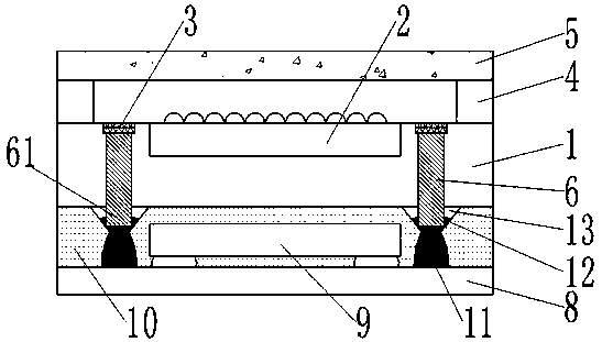
[0032] The idea of ​​the present invention is to design a camera sensing component that can improve yield rate and production efficiency. The basic idea is to use two bonding parts for thermocompression bonding and use an air gap to prevent delamination and peeling problems caused by stress. Specifically Examples will be described in the following.

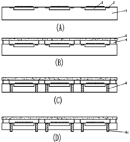
[0033] see figure 1 , the camera sensing assembly of this embodiment is obtained by bonding a first bonding portion and a second bonding portion, wherein, the first bonding portion, the first bonding portion includes a semiconductor substrate 1, a spacer 4 and cover glass 5. The semiconductor substrate 1 is a traditional silicon material, which is cut from a semiconductor wafer, and has pads 3 and sensor chip regions 2 on its upper surface, and the pads 3 are connected to the sensor chip region 2 .

[0034] The cover glass 5 is adhered on the upper surface of the semiconductor substrate 1 through the spacer 4 . Wherein, the cov...


PUM


Abstract

The invention provides a camera sensing assembly and a manufacturing method thereof. According to the camera sensing device, a first bonding part and a second bonding part are respectively manufactured, and finally the thermal compression bonding is carried out, so the production efficiency can be improved, and the problem of stress among multiple layers caused by multiple integration steps and the unreliability caused by multi-layer stacking deposition in the prior art can be avoided. Moreover, in order to reduce the bonding stress, an air gap is arranged on a bonding interface, and the air gap can prevent the solder from overflowing.

Description

technical field [0001] The invention relates to the field of packaging, testing and manufacturing of semiconductor chips, in particular to a camera sensing component and a manufacturing method thereof. Background technique [0002] Camera sensing components are the core components of camera modules, and CMOS image sensors and charge-coupled devices are currently two mainstream image sensors. Among them, the charge-coupled device is integrated on the single crystal silicon material, and the pixel signal is moved row by row and column by row and amplified accordingly at the edge exit position. The CMOS image sensor is integrated on the metal oxide semiconductor material, and each pixel has a Signal amplifier, pixel signal can be directly scanned and exported. CMOS has the advantages of low cost, simple design, small size, and low power consumption. With the maturity and progress of technology, CCD has been gradually replaced by CMOS image sensor. [0003] For existing CMOS ...

Claims


Application Information

Patent Timeline
Patent Type & Authority Applications(China)
IPC IPC(8): H01L27/146
CPCH01L27/14601H01L27/14632H01L27/14634H01L27/14643H01L27/14687H01L27/14689H01L27/1469
Inventor 侯红伟
Owner 大连环宇安迪科技有限公司
Why Eureka
Try Eureka