Supercharge Your Innovation With Domain-Expert AI Agents!

Backflow prevention circuit and power supply circuit

A reverse current prevention and power supply voltage technology, which is applied to logic circuits, circuit devices, emergency protection circuit devices, etc., can solve the problems of rising manufacturing costs of voltage regulators and inability to prevent reverse current flow.

Active Publication Date: 2019-12-31
SII SEMICONDUCTOR CORP
View PDF9 Cites 0 Cited by
  • Summary
  • Abstract
  • Description
  • Claims
  • Application Information

AI Technical Summary

Problems solved by technology

[0018] In the state of the above-mentioned formula (iii), even if the output voltage VOUT exceeds the summed value of the power supply voltage VDD and the forward voltage Vf, since the backflow prevention transistor 106 is turned on, the inflow of the backflow current cannot be prevented, and the backflow current into the voltage regulator
[0019] In order to cope with this state, in order to prevent the occurrence of the state shown in (iii) formula due to the process or temperature characteristics, it is necessary to add a process of controlling the threshold voltage VTH(inv) to be lower than the forward voltage Vf, the voltage regulation rising manufacturing costs

Method used


Image

  • Backflow prevention circuit and power supply circuit
  • Backflow prevention circuit and power supply circuit
  • Backflow prevention circuit and power supply circuit

Examples


no. 1 Embodiment approach >

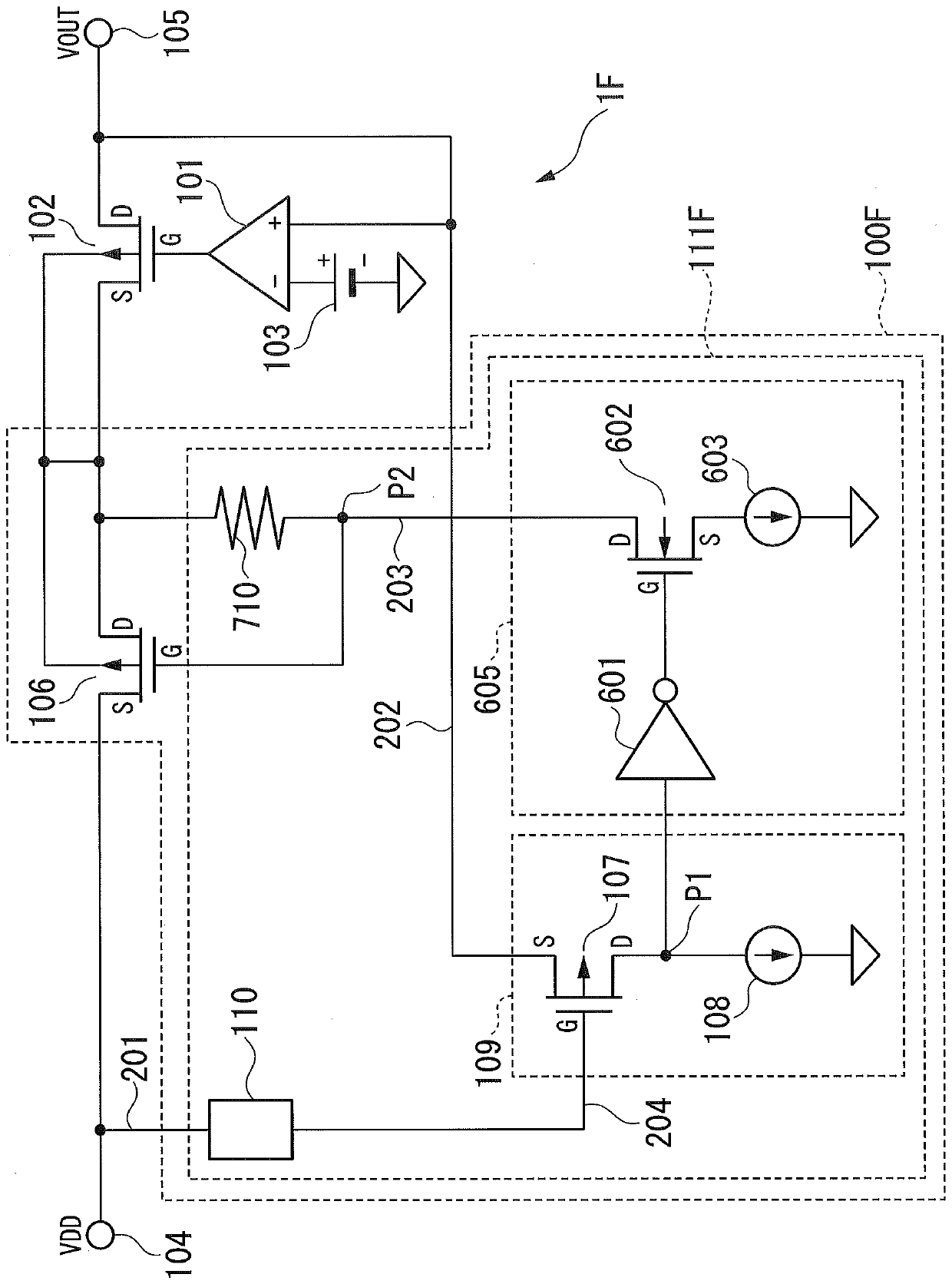
[0038] Hereinafter, a first embodiment of the present invention will be described with reference to the drawings. figure 1 It is a schematic block diagram showing a voltage regulator 1 which is a power supply circuit using the backflow prevention circuit 100 according to the first embodiment of the present invention.

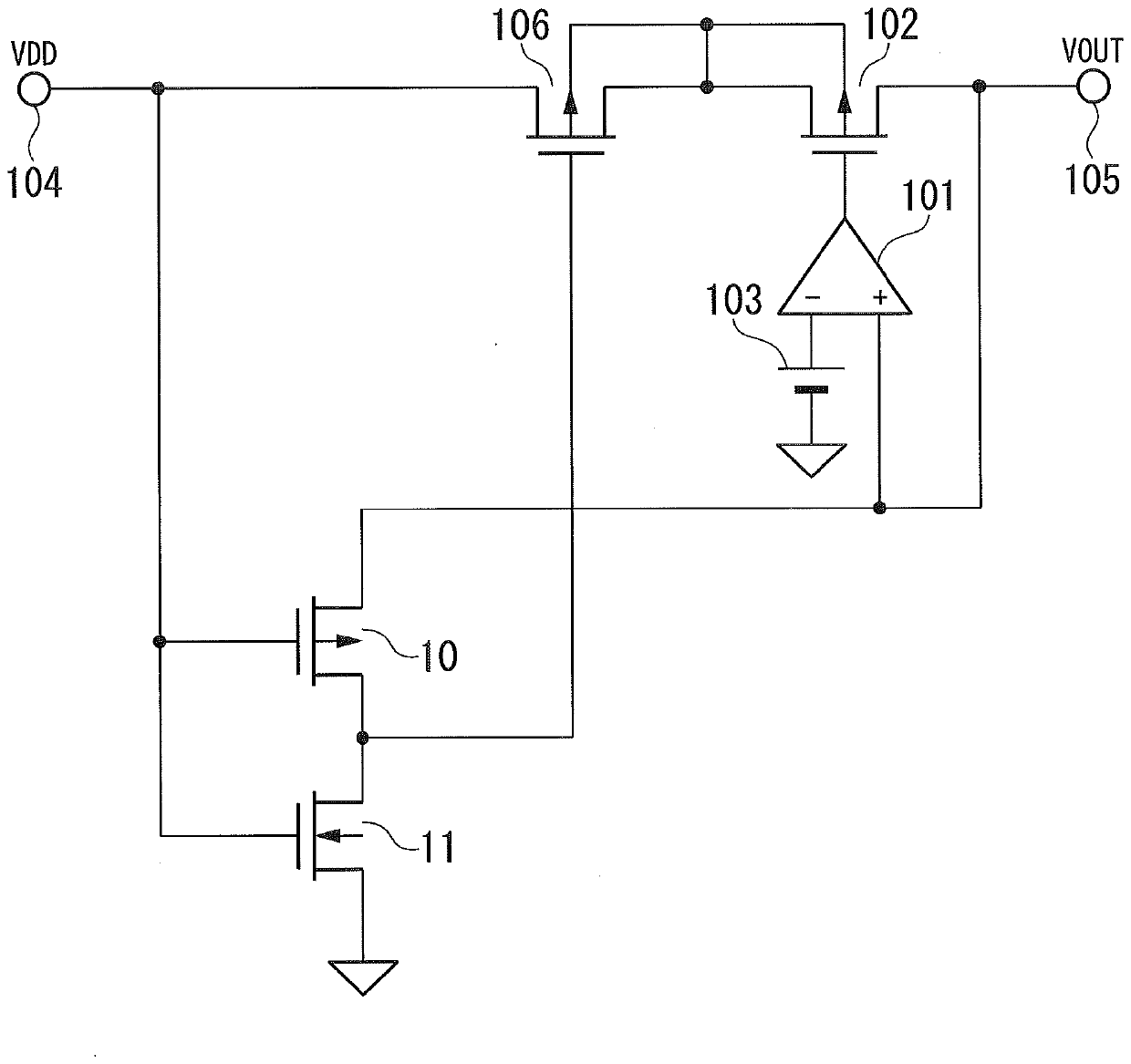
[0039] The voltage regulator 1 includes each of a backflow prevention circuit 100 , an error amplifier circuit 101 , an output stage transistor 102 , and a reference power supply 103 . The backflow prevention circuit 100 includes a backflow prevention transistor 106 and a backflow prevention control circuit 111 . The backflow prevention control circuit 111 includes a constant current inverter 109 and a level shift circuit 110 . The constant current inverter 109 includes a first transistor 107 and a constant current circuit 108 as a first constant current circuit. In the constant current inverter 109, the first transistor 107 is connected to the constant curre...

no. 2 Embodiment approach >

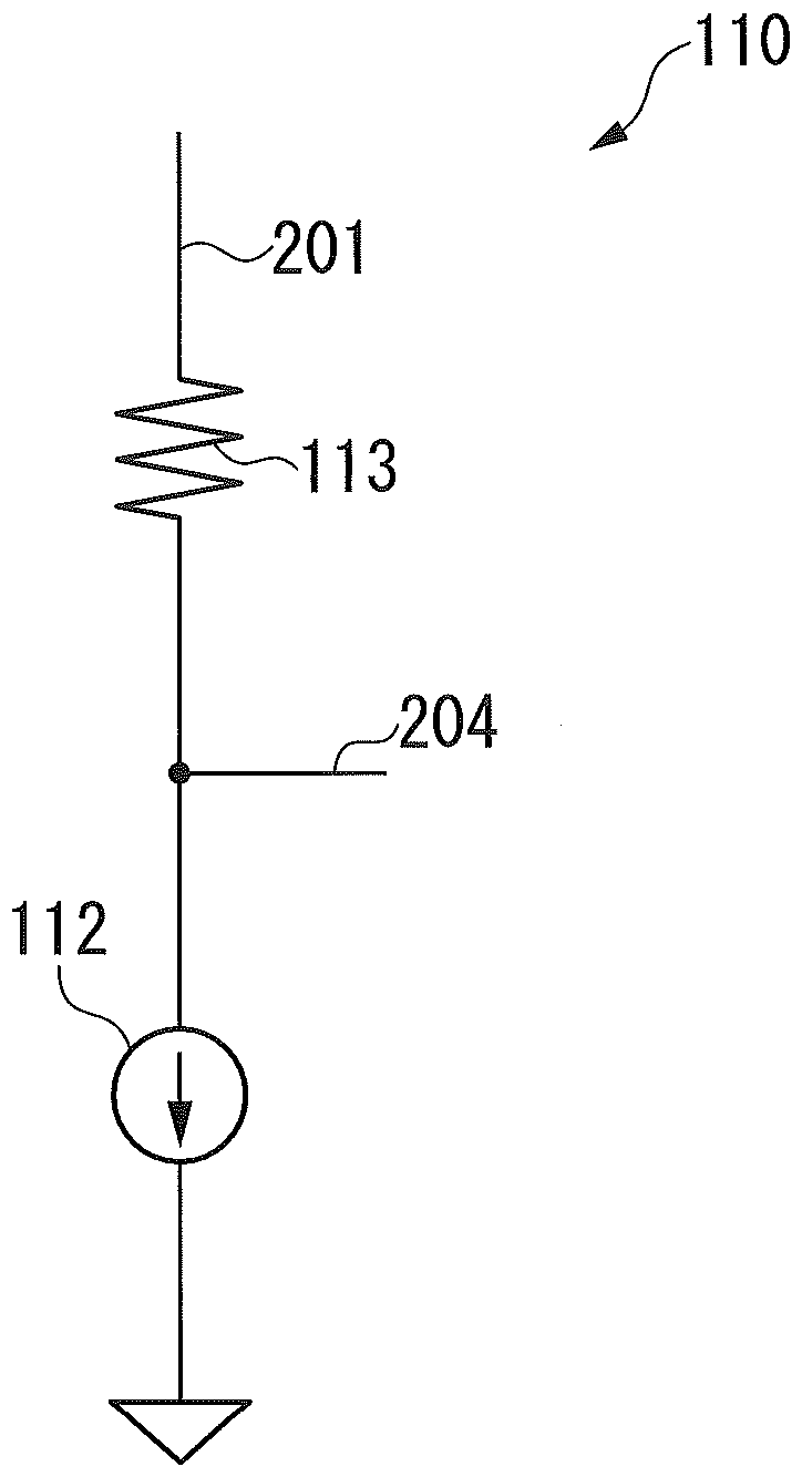
[0098] Hereinafter, a second embodiment of the present invention will be described with reference to the drawings. Figure 5 It is a diagram showing a circuit example of the level shift circuit 110A in the backflow prevention circuit 100 according to the second embodiment of the present invention. The backflow prevention circuit according to the second embodiment is configured in the same manner as the backflow prevention circuit according to the first embodiment except that a level shift circuit 110A is provided instead of the level shift circuit 110 .

[0099] The level shift circuit 110A includes a constant current circuit 112 and a PMOS transistor 114 . This PMOS transistor 114 is used instead of the resistor 113 . In addition, the constant current circuit 112 is the same as that of the first embodiment.

[0100] In the PMOS transistor 114 , the source S is connected to the wiring 201 , and the gate G and the drain D are connected to the wiring 204 .

[0101] When the c...

no. 3 Embodiment approach >

[0106] Hereinafter, a third embodiment of the present invention will be described with reference to the drawings. Figure 6 It is a diagram showing a circuit example of the level shift circuit 110B in the backflow prevention circuit 100 according to the third embodiment of the present invention. The backflow prevention circuit according to the third embodiment is configured in the same manner as the backflow prevention circuit according to the first embodiment except that a level shift circuit 110B is provided instead of the level shift circuit 110 .

[0107] The level shift circuit 110B includes a constant current circuit 112 and a diode 115 (PN junction element). In the third embodiment, instead of figure 2 Resistor 113 and diode 115 are used. The constant current circuit 112 is the same as that of the first embodiment.

[0108] In the diode 115 , the anode is connected to the wiring 201 and the cathode is connected to the wiring 204 .

[0109] In the case of the forwar...


PUM


Abstract

The present invention relates to a backflow prevention circuit and a power supply circuit. The present invention provides a reverse current prevention circuit which suppresses the influence of a process or temperature characteristics on a forward voltage of a parasitic diode of an output stage transistor (hereinafter, simply referred to as Tr) and a threshold voltage of an inverter circuit which detects an output voltage in a management process and prevents a reverse current. The disclosed device is provided with: a reverse current preventing Tr as a p-type MOSTR, which is inserted in series between an input terminal to which a power supply voltage is supplied and an output stage Tr of the p-type MOSTR from which an output voltage is output from an output terminal; and a backflow prevention control circuit which turns off the backflow prevention Tr when the output voltage exceeds the power supply voltage, the backflow prevention control unit including: the semiconductor device includesa 1st constant current circuit which is a p-type MOSTr and has a source connected to a 1st Tr of an output terminal, a drain connected to the 1st Tr and a gate of a backflow prevention Tr at one endthereof, and the other end thereof is grounded, and a level shift circuit which is inserted between an input terminal and the gate of the 1st Tr and outputs a control signal to the gate of the 1st Tr,wherein on / off control of the backflow prevention Tr is performed using a drain voltage of the 1st Tr.

Description

technical field [0001] The present invention relates to a reverse current prevention circuit and a power supply circuit. Background technique [0002] A step-down voltage regulator is used when the input voltage is higher than the output voltage. However, depending on usage conditions and circuit configurations, there are cases where the output voltage is higher than the input voltage. In this case, there is a possibility that the current flows backward from the output terminal. [0003] Therefore, even if the output voltage is higher than the input voltage, there is a p-channel MOS (metal oxide semiconductor, metal oxide semiconductor) transistor (hereinafter referred to as a PMOS transistor) that does not flow reverse current to the output stage of the voltage regulator, When the sensing output voltage is higher than the input voltage, the p-channel MOS transistor is also turned off. This structure is described in, for example, Japanese Patent Application Laid-Open No. ...

Claims


Application Information

Patent Timeline
Patent Type & Authority Applications(China)
IPC IPC(8): G05F1/56
CPCG05F1/56H03K19/018507H02H3/18H02H3/003G05F1/569
Inventor 富冈勉黑田忠克
Owner SII SEMICONDUCTOR CORP
Features
  • R&D
  • Intellectual Property
  • Life Sciences
  • Materials
  • Tech Scout
  • Unparalleled Data Quality
  • Higher Quality Content
  • 60% Fewer Hallucinations
Learn More