Semiconductor device

A semiconductor and equipment technology, applied in the field of semiconductor equipment, can solve problems such as poor film uniformity, unsuitable for large-size wafer production, and cumbersome process

Pending Publication Date: 2020-01-03
SHENZHEN JING XIANG TECH CO LTD
View PDF0 Cites 2 Cited by
  • Summary
  • Abstract
  • Description
  • Claims
  • Application Information

AI Technical Summary

Problems solved by technology

However, the uniformity of the film after direct sputtering is poor, so that follow-up processing is required in the next step, the process is cumbersome, and it is not suitable for the production of large-sized wafers

Method used


Image

  • Semiconductor device
  • Semiconductor device
  • Semiconductor device

Examples


Embodiment Construction

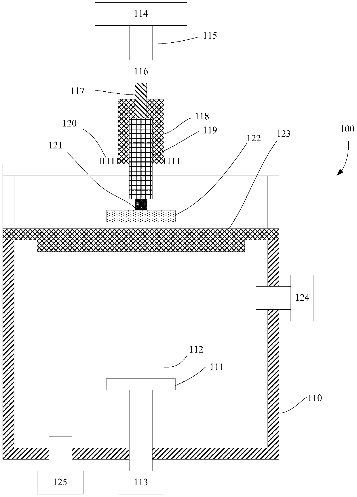
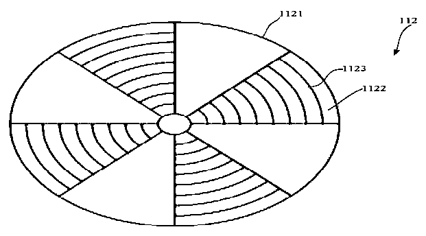
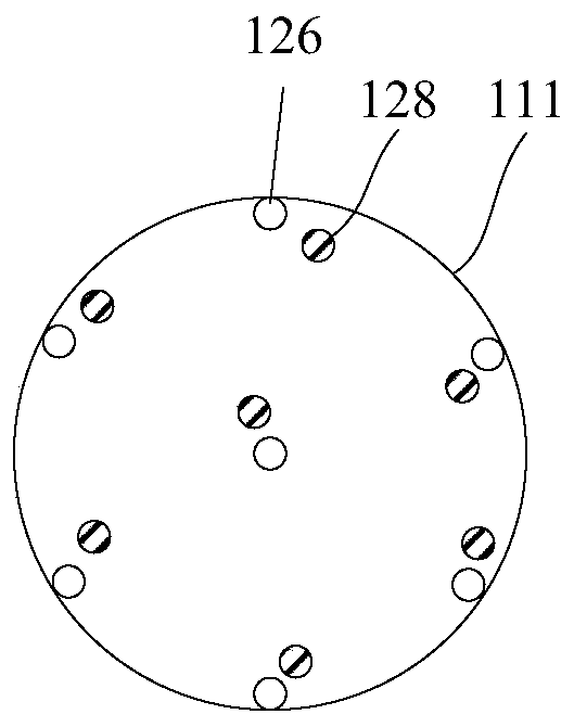
[0063] Embodiments of the present invention are described below through specific examples, and those skilled in the art can easily understand other advantages and effects of the present invention from the content disclosed in this specification. The present invention can also be implemented or applied through other different specific implementation modes, and various modifications or changes can be made to the details in this specification based on different viewpoints and applications without departing from the spirit of the present invention.

[0064] It should be noted that the diagrams provided in this embodiment are only schematically illustrating the basic idea of ​​the present invention, and only the components related to the present invention are shown in the diagrams rather than the number, shape and shape of the components in actual implementation. Dimensional drawing, the type, quantity and proportion of each component can be changed arbitrarily during actual impleme...


PUM

PropertyMeasurementUnit
surface areaaaaaaaaaaa
thicknessaaaaaaaaaa

Abstract

The invention provides a semiconductor device. The semiconductor device comprises a growth cavity, a base, a target material and a magnet, wherein the base is arranged in the growth cavity, and a substrate is allowed to be placed on the base; the target material is arranged in the growth cavity; the magnet is arranged at the position opposite to the target material; the magnet comprises a plurality of magnetic units, and the magnet forms an arc-shaped magnetic field. The semiconductor device can improve the coating uniformity.

Description

technical field [0001] The invention relates to the field of semiconductors, in particular to a semiconductor device. Background technique [0002] With the continuous advancement of integrated circuit production technology, the integration level of circuit chips has been greatly improved. At present, the number of transistors integrated in a chip has reached an astonishing tens of millions, and the signal integration of such a large number of active components requires more than ten layers of high-density metal interconnection layers for connection. Therefore, as an important process for preparing the above-mentioned metal interconnection layer, physical vapor deposition (Physical Vapor Deposition, hereinafter referred to as PVD) technology has been widely used. [0003] In the magnetron sputtering equipment, electrons are accelerated to the substrate under the action of an electric field, during which they collide with argon atoms, ionize a large number of argon ions and ...

Claims


Application Information

Patent Timeline
Patent Type & Authority Applications(China)
IPC IPC(8): C23C14/35C23C14/56C23C14/50C23C14/54C23C14/06
CPCC23C14/35C23C14/3407C23C14/566C23C14/50C23C14/505C23C14/542C23C14/541C23C14/0617H01L33/04H01L33/32H01L33/0075
Inventor 林信南游宗龙刘美华李方华児玉晃板垣克則
Owner SHENZHEN JING XIANG TECH CO LTD
Why Eureka
Try Eureka