Quantum dot display panel and display device

A technology of display panels and quantum dots, applied in nonlinear optics, instruments, optics, etc., can solve the problems of reducing device efficiency and low luminous efficiency of quantum dot materials

Active Publication Date: 2020-01-03
BOE TECH GRP CO LTD +1
View PDF9 Cites 11 Cited by
  • Summary
  • Abstract
  • Description
  • Claims
  • Application Information

AI Technical Summary

Problems solved by technology

However, in the quantum dot display panel of the prior art, the light emitted by the backlight can actually be used to excite the quantum dot mater

Method used


Image

  • Quantum dot display panel and display device
  • Quantum dot display panel and display device
  • Quantum dot display panel and display device

Examples


example 1

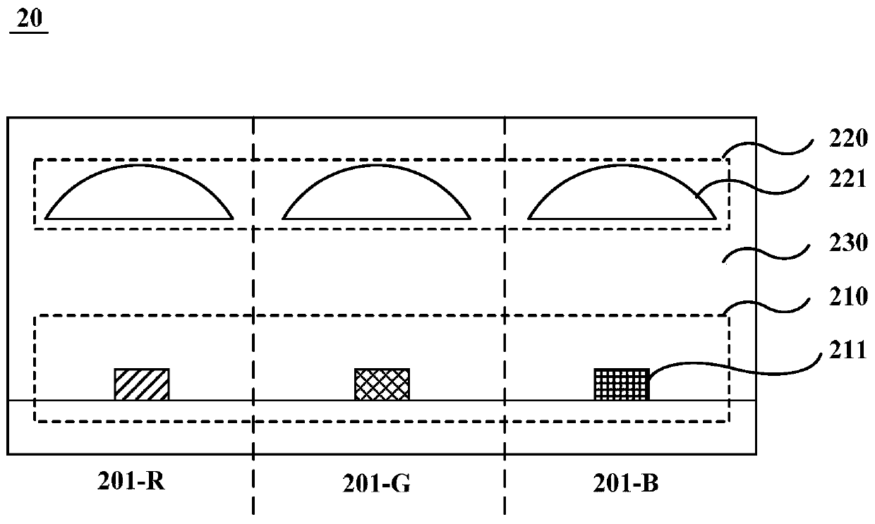
[0081] In some embodiments of the present application, such as Figure 6a As shown, the dimming layer 240 may include a second lens array 2410, the second lens array 2410 is located on the side of the first lens array 220 away from the quantum dot array 210, and includes a plurality of second lenses 2411 arranged at intervals, one second The lens 2411 is located in one sub-pixel 201 . The second lens 2411 is used for converging the incident light, and adjusting the converging point of the outgoing light under the action of the electric field.

[0082] In this way, different electric fields can be applied to the second lens 2411 in each sub-pixel 201, so that the light emitted from the second lens 2411 is refracted to different degrees and converged at different points, thereby achieving different gray scales. and display in different colors.

[0083] Such as Figure 7a As shown, when there is no electric field on the second lens 2411, the focal length of the lens is infinit...

example 2

[0129] In some embodiments of the present application, a quantum dot display panel is provided, such as Figure 15 As shown, the difference from Example 1 is that the dimming layer 240 includes a first polarizer 2460 , a plurality of first electrode layers 2431 arranged at intervals, a liquid crystal layer 30 , a second electrode layer 2440 , and a second polarizer 2480 . Each first electrode layer 2431 is located in a sub-pixel, and the second electrode 2440 applies an electric field to the liquid crystal layer 30 to change the deflection state of the liquid crystal layer 30, thereby realizing the adjustment of the refraction direction of light, so that the quantum dot display panel displays different grayscale. The first polarizer 2460 is arranged on the side of the array control layer 2450 away from the liquid crystal layer 30 , and the second polarizer is arranged on the side of the second electrode 2440 away from the liquid crystal layer 30 .

[0130] In the quantum dot ...


PUM


Abstract

The invention provides a quantum dot display panel and a display device, relates to the technical field of display, and can solve a problem of low luminous efficiency of a quantum dot display device.The quantum dot display panel is provided with a plurality of sub-pixels. The quantum dot display panel comprises a quantum dot array, a first lens array and a dimming layer. The quantum dot array comprises a plurality of quantum dot luminous layers arranged at intervals, wherein one quantum dot luminous layer is arranged in one sub-pixel. The first lens array is arranged on the light emitting side of the quantum dot array and comprises a plurality of first lenses arranged at intervals. One lens is arranged in one sub-pixel, and the first lens is used for emitting parallel light. The dimming layer is arranged on the light emitting side of the first lens array and is provided with a plurality of dimming regions with adjustable transmittance. One dimming region is arranged in one sub-pixel.The display device comprises the quantum dot display panel provided by the invention.

Description

technical field [0001] The present application relates to the field of display technology, in particular to a quantum dot display panel and a display device. Background technique [0002] Quantum dot display panels have the advantages of high color gamut, low energy consumption, and adjustable spectrum, and are used more and more widely. However, in the quantum dot display panel of the prior art, the light emitted by the backlight source can actually be used to excite the quantum dot material to emit less light, which leads to the problem of low luminous efficiency of the quantum dot material and reduces the efficiency of the device. Contents of the invention [0003] Embodiments of the present application provide a quantum dot display panel and a display device. The luminous efficiency of the quantum dot display panel can be improved. [0004] In order to achieve the above object, embodiments of the present invention adopt the following technical solutions: [0005] Th...

Claims


Application Information

Patent Timeline
IPC IPC(8): G02F1/13357G02F1/1335G02F1/1347G02F1/15
CPCG02F1/1336G02F1/133606G02F1/133514G02F1/133526G02F1/1347G02F1/15G02F1/133607G02F1/133614
Inventor 杨松祝明刘玉杰张世玉石戈方正孙艳六
Owner BOE TECH GRP CO LTD
Why Eureka
Try Eureka