Magnetic random access memory with error correction and compression circuit

A random access memory and magnetic technology, applied in the field of storage devices and magnetic random access memory, can solve the problems of long read and write delay and low performance, and achieve the effect of reducing read and write, improving performance and durability, and solving the problem of data errors.

Active Publication Date: 2020-01-07
SHANGHAI CIYU INFORMATION TECH
View PDF14 Cites 4 Cited by
  • Summary
  • Abstract
  • Description
  • Claims
  • Application Information

AI Technical Summary

Problems solved by technology

[0009] In view of the above-mentioned defects of the prior art, the technical problem to be solved by the present invention is: the error correction circuit, compression and decompression circuit in the prior art have long read and write delays and low performance

Method used


Image

  • Magnetic random access memory with error correction and compression circuit
  • Magnetic random access memory with error correction and compression circuit
  • Magnetic random access memory with error correction and compression circuit

Examples


Embodiment Construction

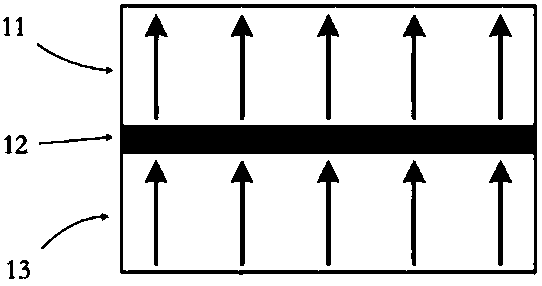
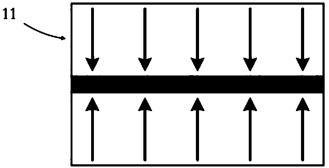
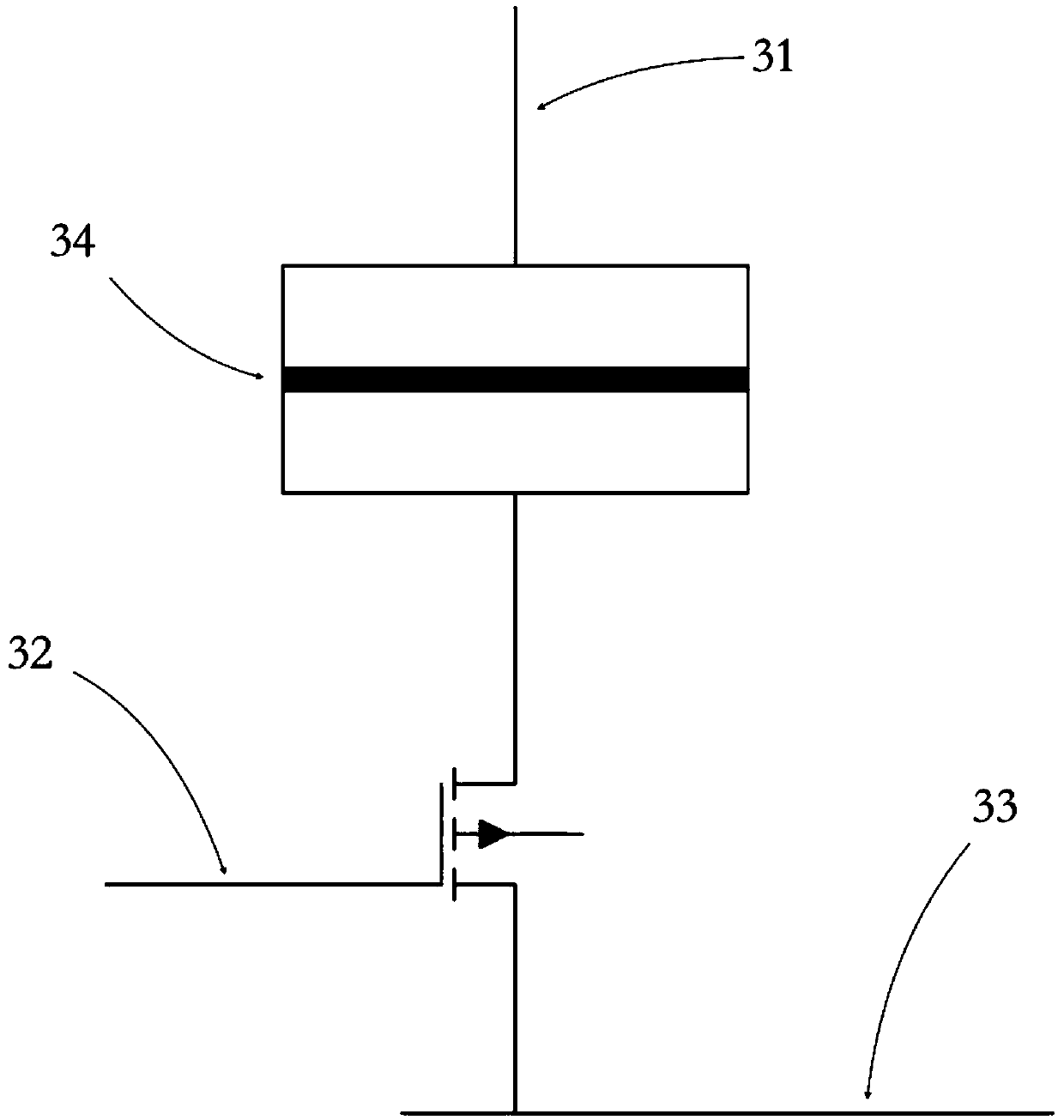
[0027] In order to make the above objects, features and advantages of the present invention more comprehensible, specific implementations of the present invention will be described in detail below in conjunction with the accompanying drawings. It should be noted that all the drawings of the present invention are in simplified form and use inaccurate scales, and are only used to facilitate and clearly assist the purpose of illustrating the embodiments of the present invention.

[0028] The present invention uses the data cache (Data Cache) to temporarily save the data to be written into the MRAM array, and reads out the data in the corresponding MRAM array through the control circuit and passes through the error correction and decompression circuit, and then merges the data to be written with it New compressed data and parity bits are reproduced and written into the MRAM array. The present invention also uses the status bit cache (FlagCache) to save the status bit of the compre...


PUM


Abstract

The invention provides a magnetic random access memory with an error correction and compression circuit. The magnetic random access memory comprises a memory cell array, an error detection and correction circuit, a compression and decompression circuit, a control circuit, a status bit cache and a data cache, the reading operation steps of the chip are as follows: obtaining first compressed data inthe memory cell array, processing the first compressed data through the error detection and correction circuit, decompressing the processed first compressed data through the compression and decompression circuit to obtain first data, and outputting the first data; and the chip performs the following writing operation steps: compressing second data to be written through the compression and decompression circuit to obtain second compressed data, processing the second compressed data through the error detection and correction circuit, and writing the processed second compressed data into the memory cell array.

Description

technical field [0001] The invention relates to a storage device, in particular to a magnetic random access memory with error correction and compression circuits, and belongs to the technical field of semiconductor chips. Background technique [0002] MRAM is a new memory and storage technology that can be read and written as fast as SRAM / DRAM, and can permanently retain data after power failure like Flash memory. Its economy is quite good, and the silicon area occupied per unit capacity has a great advantage over SRAM, and also has advantages over NOR Flash, which is often used in such chips, and has greater advantages than embedded NOR Flash. Its performance is also quite good, the read and write latency is close to the best SRAM, and the power consumption is the best among various memory and storage technologies. Moreover, unlike DRAM and Flash, MRAM is not compatible with standard CMOS semiconductor processes. MRAM can be integrated into a chip with logic circuits. [...

Claims


Application Information

Patent Timeline
Patent Type & Authority Applications(China)
IPC IPC(8): G11C11/16
CPCG11C11/1653G11C11/1673G11C11/1675
Inventor 王春林戴瑾
Owner SHANGHAI CIYU INFORMATION TECH
Why Eureka
Try Eureka