Architecture for silicon photonics enabling wafer probe and test

A photonic and wafer technology, used in optical components, semiconductor/solid-state device testing/measurement, instruments, etc., can solve the problems of difficult to test optical components of photonic chips, and impossible to test optical components of photonic chips.

Active Publication Date: 2020-01-10
XILINX INC
View PDF5 Cites 12 Cited by
  • Summary
  • Abstract
  • Description
  • Claims
  • Application Information

AI Technical Summary

Problems solved by technology

However, it is difficult, if not impossible, to test the optical components in a photonic chip before it is mounted and aligned with the fiber optic cable
For example, it may not be possible to test

Method used


Image

  • Architecture for silicon photonics enabling wafer probe and test
  • Architecture for silicon photonics enabling wafer probe and test
  • Architecture for silicon photonics enabling wafer probe and test

Examples


Embodiment Construction

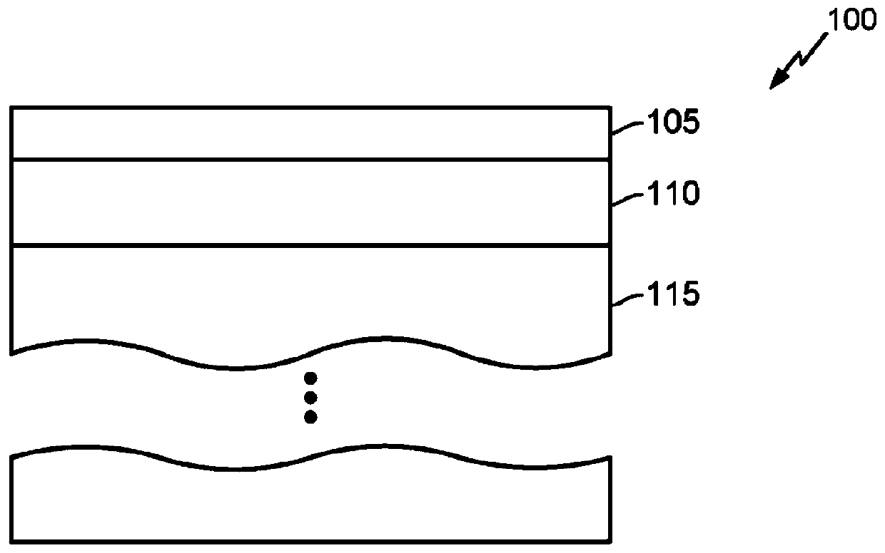
[0036] Various features are described below with reference to the accompanying drawings. It should be noted that the drawings may or may not be drawn to scale and that elements of like structure or function are represented by like reference numerals throughout the drawings. It should be noted that the drawings are only intended to facilitate the description of features. They are not intended as an exhaustive description of the specification or as a limitation on the scope of the claims. Additionally, the illustrated examples do not necessarily have all of the aspects or advantages shown. An aspect or advantage described in connection with a particular example is not necessarily limited to that example, and can be practiced in any other example even if not so shown or explicitly described.

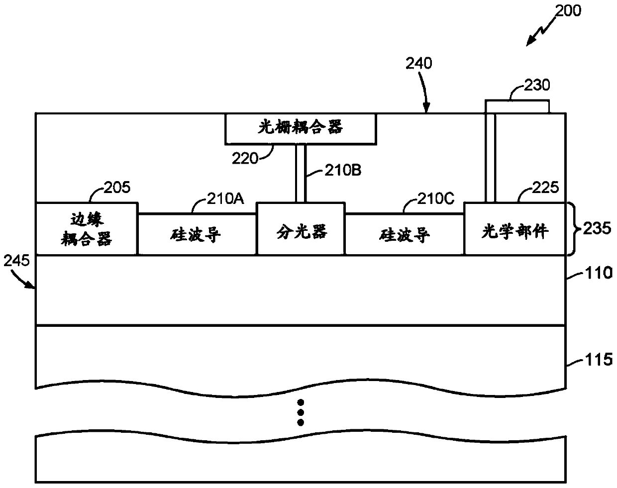
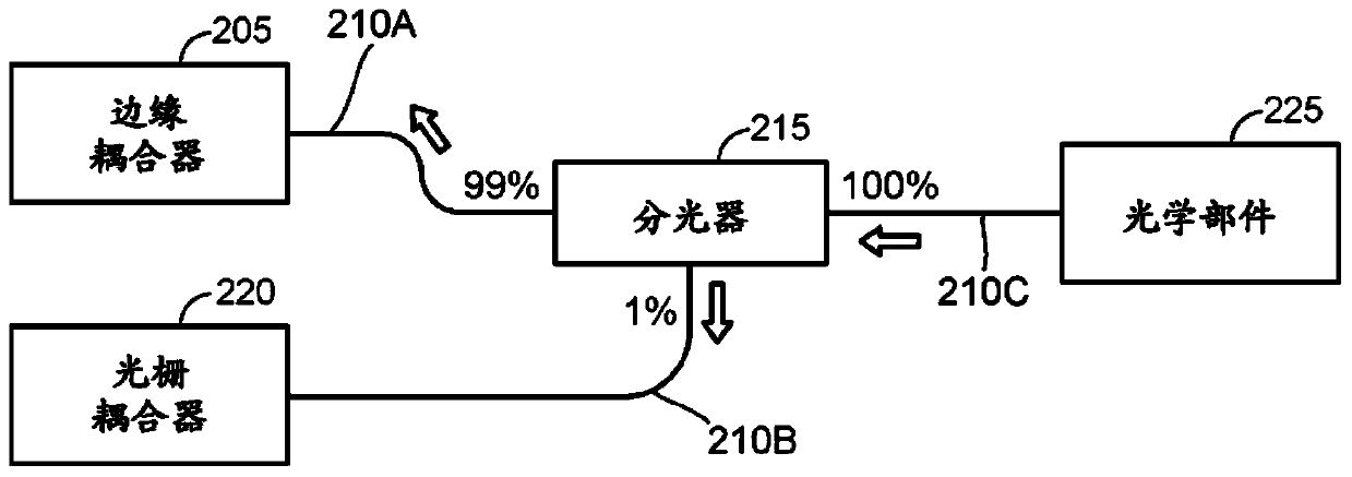
[0037] Embodiments herein describe techniques for using grating couplers to test or align optical components in photonic chips. In one embodiment, the photonic chip may include edge coup...


PUM


Abstract

Embodiments herein describe techniques for testing or aligning optical components (205, 225) in a photonic chip (200) using a grating coupler (220). In one embodiment, the photonic chip (200) may include an edge coupler (205) and a grating coupler (220) for optically coupling the photonic chip to external fiber optic cables (920). The edge coupler (205) may be disposed on a side or edge of the photonic chip while the grating coupler (220) is located on a top or side of the photonic chip. During fabrication, the edge coupler (205) may be inaccessible. Instead of using the edge coupler (205) totest the photonic chip, a testing apparatus (805) can use the grating coupler (220) along with a splitter (215) to transfer optical test signals between an optical component in the photonic chip (e.g., a modulator or detector) and a test probe (505) optically coupled to the grating coupler (220).

Description

technical field [0001] Examples of the present disclosure relate generally to testing optical components in photonic chips, and in particular, to using grating couplers to verify the functionality of optical components integrated into photonic chips. Background technique [0002] Many network devices process data at rates that cannot be achieved using conductive cables. For example, the I / O rate of a network device may mean that using conductive cables (eg, Ethernet cables) requires too much power or introduces too much noise. So, if high-speed signals need to be passed between network devices, the devices can use fiber optic cables, which can accommodate much higher data rates over greater distances than conductive cables. [0003] A network device may include one or more photonic chips coupled to an optical cable. For example, photonic chips can be coupled to hundreds of different fiber optic cables. But it is difficult, if not impossible, to test the optical components...

Claims


Application Information

Patent Timeline
IPC IPC(8): G02B6/12G02B6/124
CPCG02B6/30H01L22/12G02B6/12004G02B6/124G02B6/125G02B6/4225G02B2006/1215G02B2006/12061
Inventor A·H·莱西
Owner XILINX INC
Why Eureka
Try Eureka