Ceramic circuit board and module using same

A technology for circuit substrates and ceramic substrates, which is applied to the improvement of circuit substrate materials, circuits, and metal adhesion of insulating substrates, etc., can solve the problems such as the inability to meet the heat resistance cycle characteristics, the decrease in the continuity of the solder layer, and the increase in Vickers hardness.

Pending Publication Date: 2020-01-17
DENKA CO LTD
View PDF20 Cites 1 Cited by
  • Summary
  • Abstract
  • Description
  • Claims
  • Application Information

AI Technical Summary

Problems solved by technology

[0011] However, according to this method, although the bonding strength of the ceramic substrate interface is improved, the continuity of the brazing filler metal layer mainly composed of Ag decreases as the amount of In added increases, and the Vickers hardness also increases.
When the continuity of the solder layer decreases and the Vickers hardness increases, the buffering function for alleviating the thermal stress caused by the difference in thermal expansion coefficient at the bonding interface between the ceramic substrate and the metal plate decreases, for example, the bonding cannot be satisfied. Heat cycle resistance characteristics required for ceramic circuit boards such as 0.8mm thick copper plate

Method used


Image

  • Ceramic circuit board and module using same
  • Ceramic circuit board and module using same
  • Ceramic circuit board and module using same

Examples


Embodiment 1

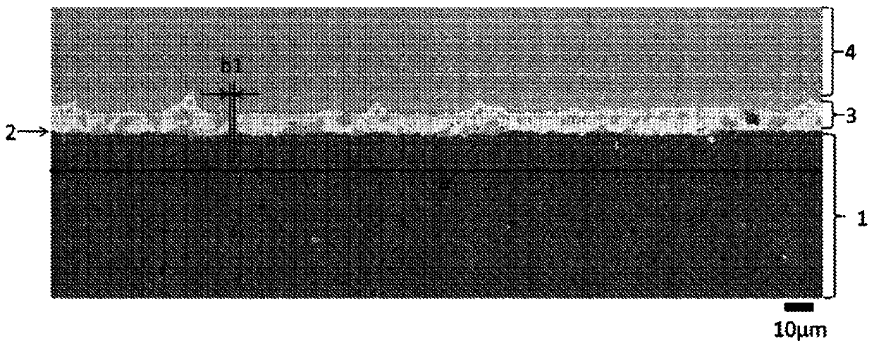
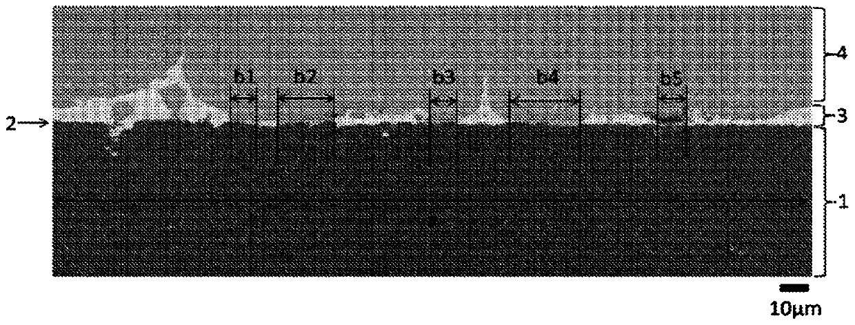
[0056] On a silicon nitride substrate with a thickness of 0.32 mm, 90 parts by mass of Ag powder (manufactured by Fukuda Metal Foil Powder Industry Co., Ltd.: Ag-HWQ2.5 μm) and Cu powder (manufactured by Fukuda Metal Foil Powder Industry Co., Ltd.: Cu -10 parts by mass of 10 parts by mass of HWQ) contains 3.5 parts by mass of TiH2 powder (manufactured by OSAKA Titanium technologies Co., Ltd.: TSH-350) and 3.5 parts by mass of Sn powder (manufactured by Fukuda Metal Foil Powder Industry Co., Ltd.: Sn-HPN 3μm) 3 parts by mass of active metal solder, at 1.0×10 -3 An oxygen-free copper plate with a thickness of 0.8 mm was bonded to the circuit surface, and an oxygen-free copper plate with a thickness of 0.8 mm was bonded to the back surface at 800° C. for 30 minutes in a vacuum below Pa.

[0057] On the bonded circuit board, a UV curable resist is printed as a circuit pattern by screen printing, and after UV curing, the shape of the heat dissipation surface is further printed and ...

Embodiment 2~10、 comparative example 1~7

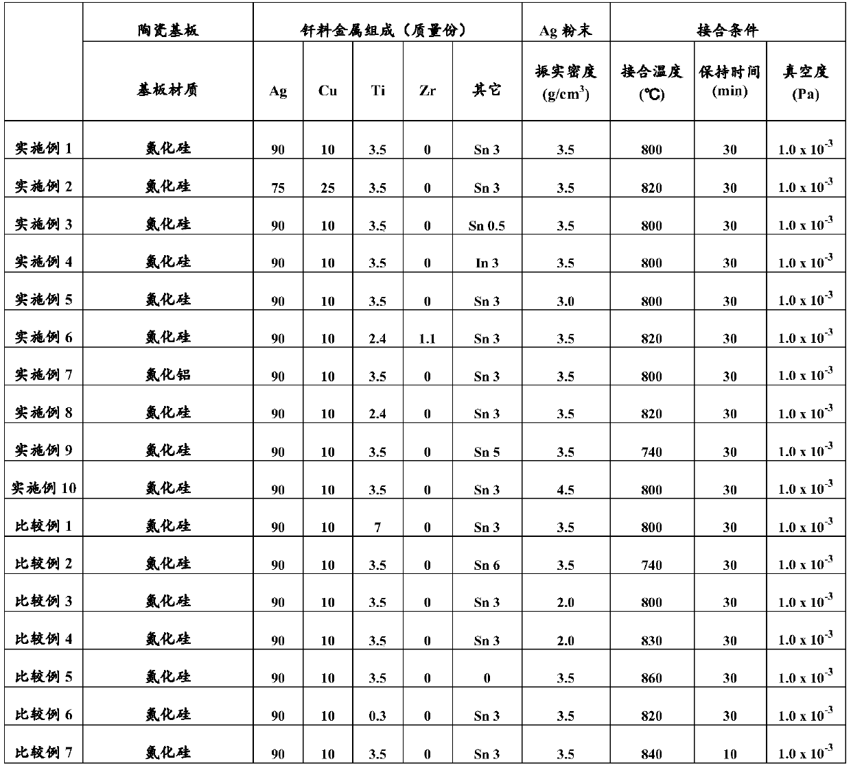
[0066] Except having set the conditions shown in Table 1, it carried out similarly to Example 1. The evaluation results are shown in Table 2.

[0067] 【Table 1】

[0068]

[0069] 【Table 2】

[0070]

[0071]

[0072] As shown in Table 2, regarding the use of a tap density of 3 g / cm 3 The above-mentioned Ag powder, the addition amount of In or Sn is 5 parts by mass or less, and the ceramic circuit board produced under the conditions of the bonding temperature is 820 ° C or less. It is confirmed that the Vickers hardness of the solder layer is in the range of 60 to 85 Hv. The occurrence rate of horizontal cracks after the cycle test is less than 1%. Regarding the circuit board produced under the condition that the addition amount of Sn is 3 parts by mass or less and the bonding temperature is 800° C. or less, it was confirmed that the Vickers hardness was in the range of 60 to 75 Hv, and the continuity rate of the solder layer was also 90% or more. The occurrence rat...


PUM

PropertyMeasurementUnit
Vickers hardnessaaaaaaaaaa
thicknessaaaaaaaaaa
densityaaaaaaaaaa

Abstract

An aim of the invention is to provide a ceramic circuit board having good bonding characteristics and excellent heat-resistant cycle characteristics. [Solution] A ceramic circuit board characterized in that: a ceramic substrate and a copper plate are bonded with a brazing material, the brazing material containing Ag, Cu, at least one active metal component selected from among Ti and Zr, and at least one element selected from among In, Zn, Cd, and Sn; the continuity ratio of the brazing material layer after bonding is at least 80%; and the Vickers hardness of the brazing material layer is 60-85Hv.

Description

technical field [0001] The present invention relates to a ceramic circuit substrate and a module using the same. Background technique [0002] As circuit substrates used in power modules and the like, ceramic substrates such as alumina, beryllium oxide, silicon nitride, and aluminum nitride are used from the viewpoints of thermal conductivity, cost, and safety. These ceramic substrates are used as circuit boards by joining metal circuit boards such as copper and aluminum and radiator plates. These resin substrates and metal substrates with resin layers as insulating materials have excellent insulation and heat dissipation properties, and therefore are used as substrates for mounting high heat dissipation electronic components. [0003] For power modules such as elevators, vehicles, and hybrid vehicles, ceramic circuit boards are used in which metal circuit boards are bonded to the surface of ceramic substrates with solder, and semiconductor elements are mounted on predeterm...

Claims


Application Information

Patent Timeline
Patent Type & Authority Applications(China)
IPC IPC(8): C04B37/02B23K35/30C22C5/06H01L23/14H05K1/03H05K3/38
CPCB23K35/30C04B37/02H01L23/14H05K1/03H05K3/38C22C5/06C04B2237/407C04B2237/125C04B2237/127C04B2237/706C04B2237/368C04B2237/366C04B37/026H05K1/0306H05K3/381H01L23/15B23K2101/42B23K1/0016B23K35/3006C04B37/023C22C5/08Y10T428/12875
Inventor 津川优太西村浩二原田祐作青野良太岩切翔二
Owner DENKA CO LTD
Why Eureka
Try Eureka