Semiconductor element, semiconductor package structure and manufacturing method thereof

A technology of packaging structure and manufacturing method, which is applied in semiconductor/solid-state device manufacturing, semiconductor devices, semiconductor/solid-state device components, etc., and can solve problems affecting bonding effects, heat dissipation effects, and high temperature

Active Publication Date: 2013-12-11
ADVANCED SEMICON ENG INC
View PDF4 Cites 5 Cited by
  • Summary
  • Abstract
  • Description
  • Claims
  • Application Information

AI Technical Summary

Problems solved by technology

It is known that several material combinations of the backside metallization and the thermal interface material have been proposed. However, in the current known technology, voids (voids) will inevitably be generated in

Method used


Image

  • Semiconductor element, semiconductor package structure and manufacturing method thereof
  • Semiconductor element, semiconductor package structure and manufacturing method thereof
  • Semiconductor element, semiconductor package structure and manufacturing method thereof

Examples


Embodiment Construction

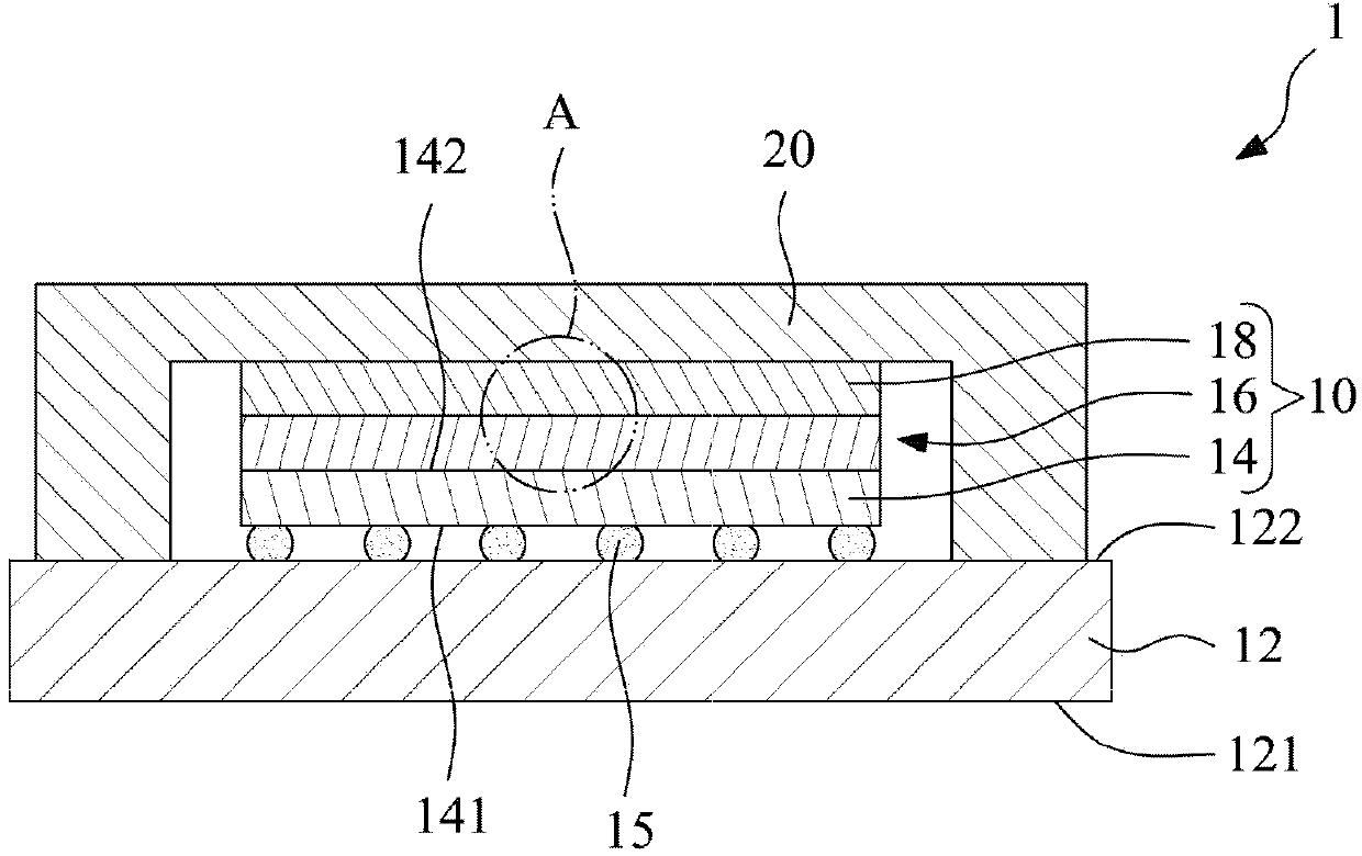
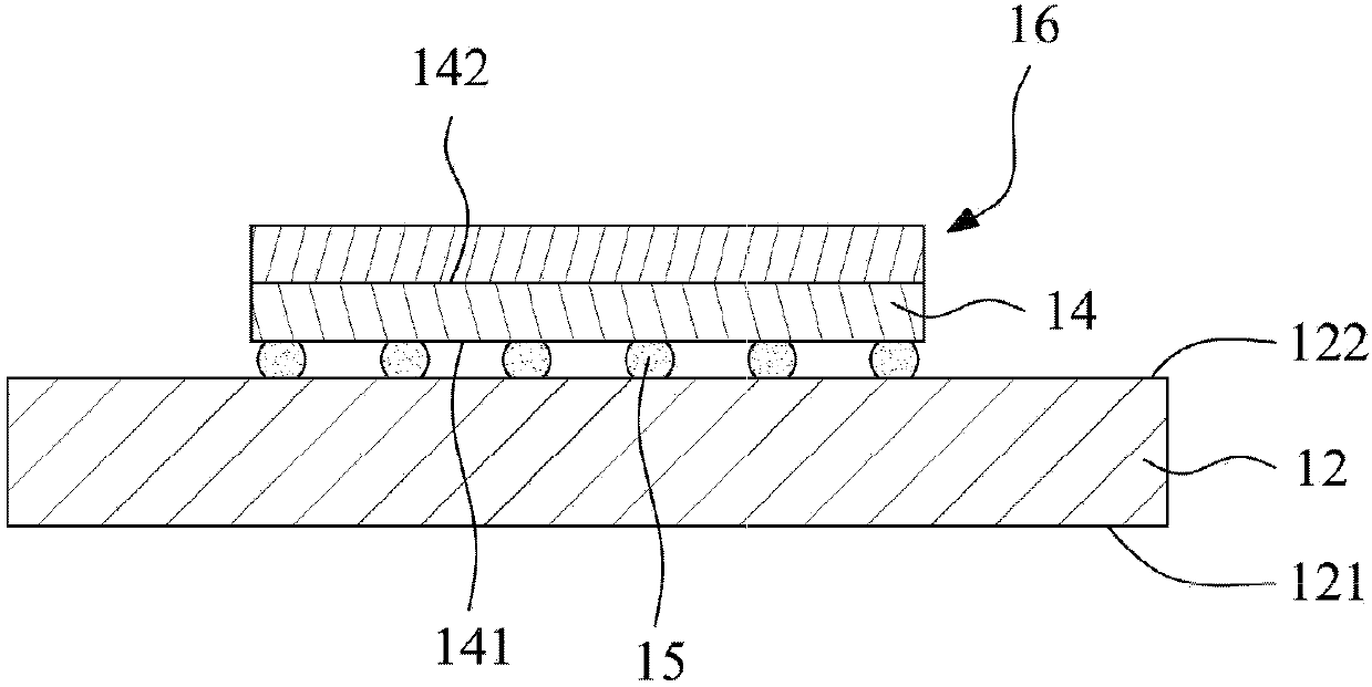
[0017] refer to figure 1 , shows a schematic cross-sectional view of an embodiment of the semiconductor package structure of the present invention. The semiconductor package structure 1 includes a substrate 12 , a semiconductor element 10 and a heat sink 20 . The substrate 12 is a packaging substrate, which includes a first surface 121 , a second surface 122 and several internal electrical connection elements (not shown in the figure). The internal electrical connection elements are used to electrically connect the first surface 121 and the second surface 122 .

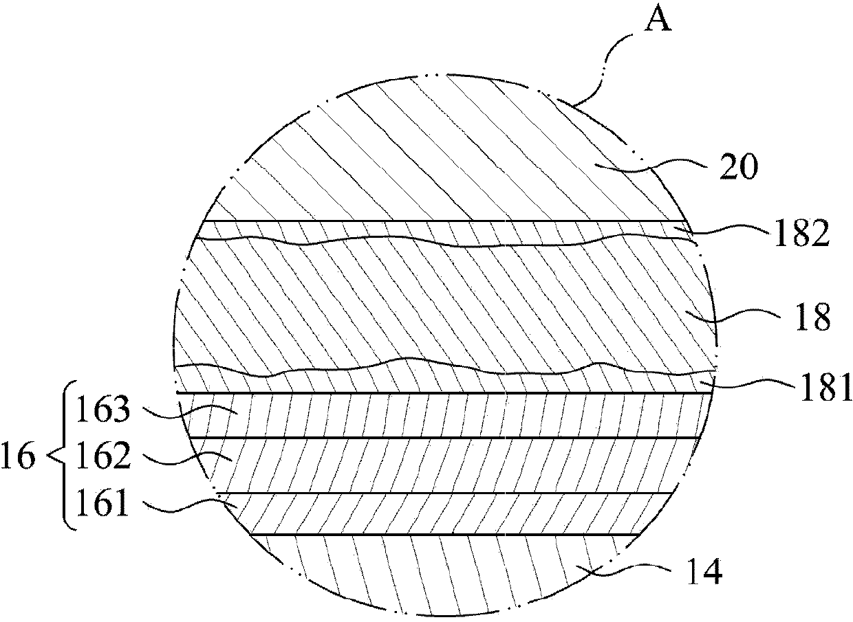
[0018] The semiconductor device 10 includes a semiconductor die 14 , several bumps 15 , a back side metallization (BSM) 16 and a thermal interface material 18 .

[0019] The semiconductor die 14 includes a first surface 141 and a second surface 142 .

[0020] The bumps 15 are located on the first surface 141 of the semiconductor die 14 and electrically connect the first surface 141 of the semiconductor die 14 to th...


PUM

PropertyMeasurementUnit
Thicknessaaaaaaaaaa

Abstract

The invention relates to a semiconductor element, a semiconductor package structure and a manufacturing method thereof. The semiconductor device includes a semiconductor crystal, a back side metal coating, a thermal interface material and a first intermetallic compound. The back side metal coating is arranged on one surface of the semiconductor crystal. The thermal interface material is arranged on the back side metal coating and contains indium zinc alloy. The first intermetallic compound is arranged between the back side metal coating and the thermal interface material, contains indium and does not contain zinc. Therefore, during the reflow process, the bonding effect and heat radiating effect are increased.

Description

technical field [0001] The invention relates to a semiconductor element, a semiconductor packaging structure and a manufacturing method thereof. Specifically, the present invention relates to a semiconductor device with Back Side Metallization (BSM) and Thermal Interface Material (TIM), a semiconductor package structure and a manufacturing method thereof. Background technique [0002] In the known semiconductor package structure, a heat sink is usually covered to contact the backside of the chip on the substrate and dissipate the heat generated by the chip. Since the heat sink is made of copper and the chip is made of silicon, the bonding effect and heat dissipation effect of the two are not good. In order to improve the above shortcomings, one solution is to add Back Side Metallization (BSM) and Thermal Interface Material (TIM) on the back of the chip, and the heat sink first contacts the thermal interface material, and then The heat sink is bonded to the thermal interfac...

Claims


Application Information

Patent Timeline
IPC IPC(8): H01L23/373H01L23/31H01L21/48
CPCH01L2224/16225H01L2224/73253H01L2224/83101H01L2924/16152
Inventor 萧友享杨秉丰李长祺
Owner ADVANCED SEMICON ENG INC
Why Eureka
Try Eureka