Wafer structure with buffer layer

A buffer layer and wafer technology, applied in electrical components, electrical solid-state devices, circuits, etc., can solve the problems of poor product yield, lack of resistance, lead-free solder ball cracking, etc., to enhance structural strength and The effect of shock absorption and enhanced bonding ability

Active Publication Date: 2008-08-27
ADVANCED SEMICON ENG INC
View PDF0 Cites 6 Cited by
  • Summary
  • Abstract
  • Description
  • Claims
  • Application Information

AI Technical Summary

Problems solved by technology

[0006] First: Since the conductive bumps disposed on the UBM layer 112 are usually made of lead-free solder balls, and the material of tin is generally hard and brittle, the shock absorption ability is poor during the drop test. , it is easy to cause lead-free solder balls to break
This problem will cause the wafer structure to have poor shock resistance characteristics, not have good resistance to external force, and be easily damaged by collision
[0007] Second: The conductive bumps used to electrically connect the wafer and the substrate are easy to fall off from the UBM layer 112, resulting in poor product yield during the flip-chip bonding process

Method used


Image

  • Wafer structure with buffer layer
  • Wafer structure with buffer layer
  • Wafer structure with buffer layer

Examples


Embodiment Construction

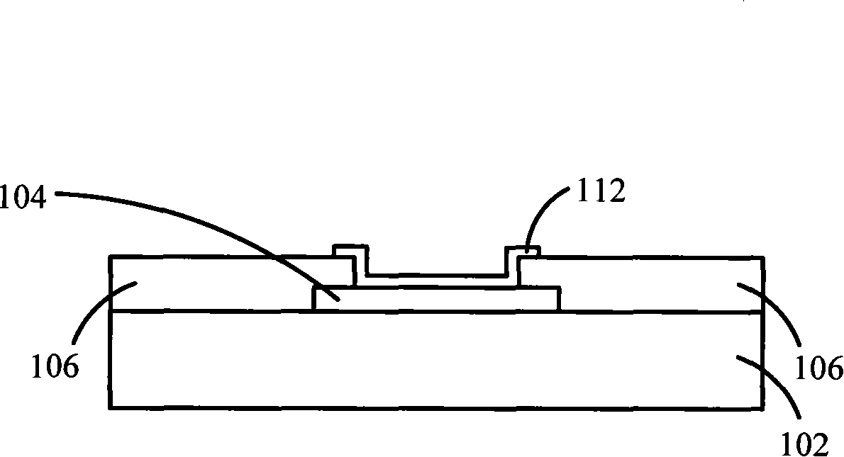
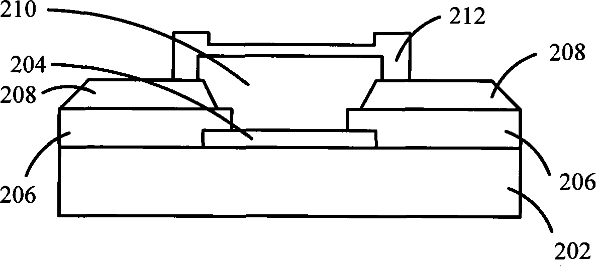
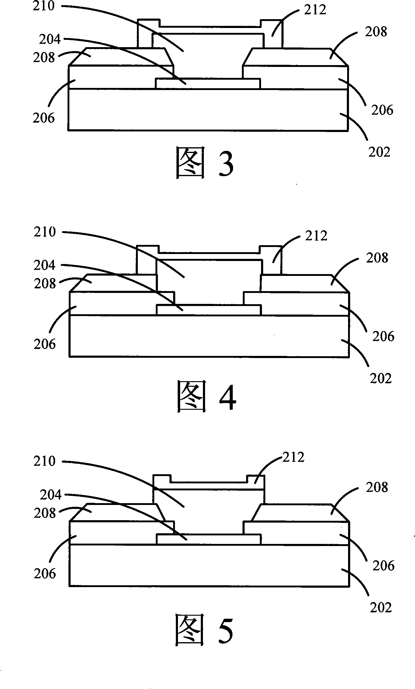
[0026] The present invention provides a wafer structure with a buffer layer, which is to add a buffer layer in the wafer structure to enhance the structural strength of the wafer and prevent the solder balls from falling off. Please refer to figure 2 The schematic diagram of the wafer structure according to the first embodiment of the present invention is shown, the wafer structure includes: a wafer 202, a protective layer 206, an outer buffer layer 208, an inner buffer layer 210 and an under-bump metal layer 212 .

[0027] Wafer 202 has a first surface (such as figure 2 The upper surface shown in ), at least one pad 204 is arranged on the first surface to form an electrical connection with the wafer 202, although only one pad 204 is shown in the figure, it should be known that the wafer A plurality of welding pads 204 may be provided on the first surface of the 202, or other electrical connection elements or other electronic / electrical elements, and these are technologies ...


PUM


Abstract

The invention discloses a wafer structure provided with a buffer layer, comprising a wafer which is provided with at least one welded gasket, wherein, a passivation layer is arranged on the wafer and exposes the welded gasket; the buffer layer is arranged on the passivation layer and the welded gasket; an under bump metallurgy (UBM) layer is arranged on the buffer layer. The buffer layer comprises a thickened inner buffer layer which is made of aluminum materials and is formed between the UBM layer and the welded gasket so as to strengthen the damping capacity of the wafer during the process of a drop test, thereby the phenomenon that a conductive lug which is used for being coupled with a substrate is dropped off and broken is avoided and the coupling ability of the conductive lug and the UBM layer can be strengthened. Moreover, the buffer layer can also comprise an outer buffer layer which is made of polyamide materials, arranged on the passivation layer and partially positioned between the UBM layer and the passivation layer.

Description

technical field [0001] The present invention relates to a wafer structure, and in particular to a wafer structure with a buffer layer, which is to add a buffer layer on the pad of the wafer to enhance the structural strength of the wafer and prevent conduction. The bump falls off, and the joining ability between the solder pad and the metal layer under the bump is strengthened. Background technique [0002] In the semiconductor packaging process, there are three commonly used methods: wire bonding, tap automated bonding and flip chip. In order to meet the requirements of today's electronic products, thin and short, It is necessary to continuously develop chips with small size and high number of pins. However, products packaged by wire bonding and tape-and-roll automatic bonding are not only relatively large in size, but also unable to meet the requirements of high number of pins. , Inverted crystal bonding has become a better choice. [0003] figure 1 shows a schematic di...

Claims


Application Information

Patent Timeline
Patent Type & Authority Applications(China)
IPC IPC(8): H01L23/485
CPCH01L2224/13
Inventor 黄泰源陈知行
Owner ADVANCED SEMICON ENG INC
Why Eureka
Try Eureka