Preparation method of low-loss infrared high-nonlinearity optical waveguide

A highly nonlinear and optical waveguide technology, applied in the field of micro-nano processing and nonlinear optics, can solve the problems of large scattering, transmission band limitation, and application performance limitation, and achieve the effect of low roughness and low loss transmission

Inactive Publication Date: 2020-01-24
SUN YAT SEN UNIV
View PDF8 Cites 4 Cited by
  • Summary
  • Abstract
  • Description
  • Claims
  • Application Information

AI Technical Summary

Problems solved by technology

[0003] At present, the main materials used for on-chip infrared waveguides include germanium, silicon, and chalcogenides. Among them, germanium waveguides not only have a large loss in infrared waveguides, but also have a transmission band mainly after 3 μm, excluding communication bands, while silicon waveguides have serious two-photon In addition to large absorption and loss, there are also problems such as transmission band restrictions and difficulty in preparation
[0004] Chalcogenide waveguide is an amorphous material formed by covalent bonds of sulfur, selenium, tellurium and some other metal and non-metallic materials, which has a very wide transmission band (fro

Method used


Image

  • Preparation method of low-loss infrared high-nonlinearity optical waveguide
  • Preparation method of low-loss infrared high-nonlinearity optical waveguide
  • Preparation method of low-loss infrared high-nonlinearity optical waveguide

Examples


Embodiment 1

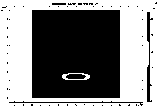
[0026] Such as Figure 4 shown, combined with Figures 1 to 5 Describe this embodiment, such as figure 1 As shown, the low-loss infrared chalcogenide optical waveguide includes: substrate silicon 201, lower cladding 202, fiber core 203, and upper cladding 204 from bottom to top; the lower cladding 202 is silicon dioxide; The core 203 on the cladding layer 202 cladding and having an incident surface and an exit surface is an infrared chalcogenide; and at least the upper cladding 204 embedded in these cores 203 is air; the refractive index of the core 203 is larger than that of the upper and lower claddings. , and the interfaces between the core 203 and the upper cladding 204 and the lower cladding 202 are smooth.

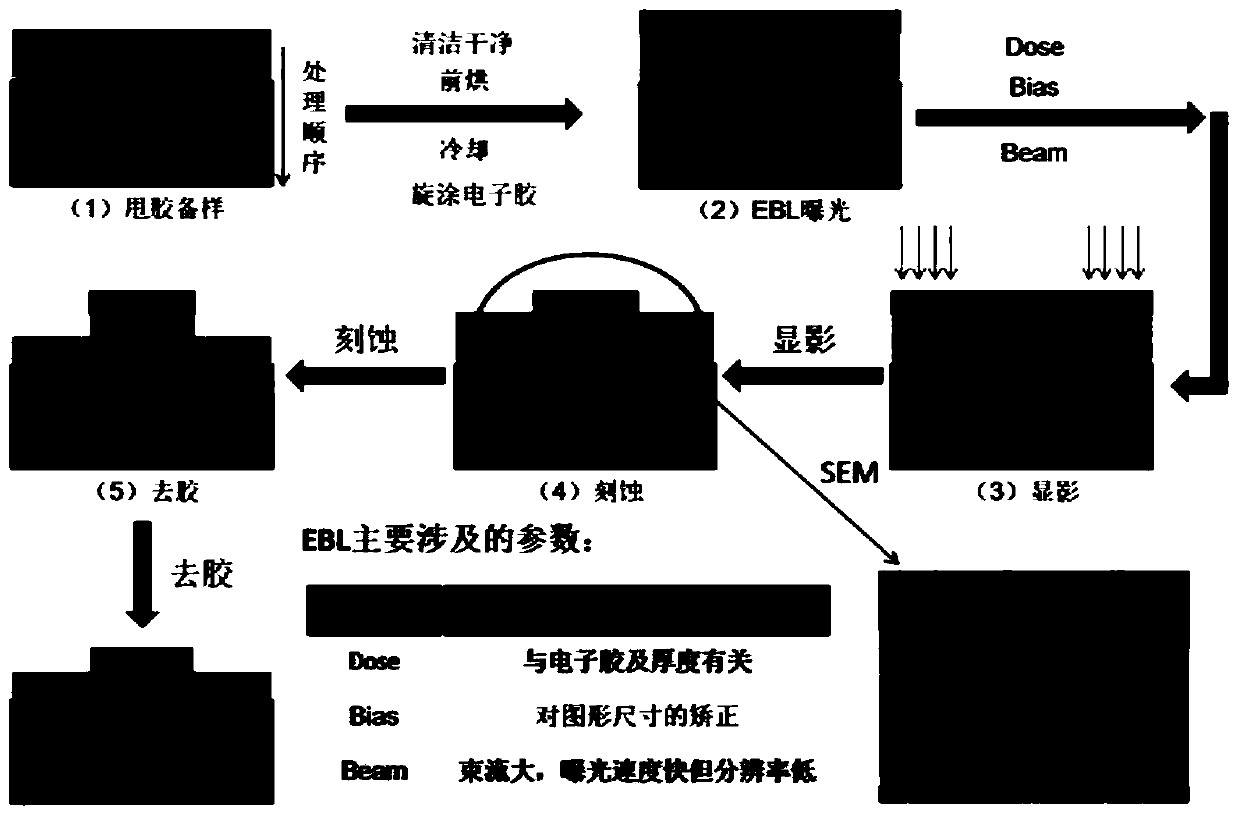
[0027] This embodiment provides a method for preparing a low-loss infrared chalcogenide waveguide, which relates to the fields of micro-nano processing and nonlinear optics, especially the transmission of low-loss light waves in waveguides. transmission characteri...

Embodiment 2

[0040] combine Figure 5 This embodiment is described. In this embodiment, the waveguide loss coefficient is obtained by comparing the input and output powers of waveguides with different lengths, and then using the difference between the output powers of two waveguides with different lengths.

[0041] The test program for the test system for waveguide loss factor consists of the following steps:

[0042] Step 1: First, place the prepared waveguide structure on an adsorption table to ensure that the structure will not shake during the test.

[0043] Step 2: Pass the lens fiber through the three-dimensional adjustment frame, roughly align it with the input and output ends of the waveguide, observe through the CCD, and then input a beam of infrared band and 10dBm light source at the input end, and connect a power meter at the output end. And through the fine adjustment of the three-dimensional adjustment frame, the lens fiber can be aligned with the input and output ports of th...


PUM

PropertyMeasurementUnit
Section widthaaaaaaaaaa

Abstract

The invention relates to the field of micro-nano machining for on-chip waveguides, in particular to a preparation method of a low loss infrared high-nonlinearity optical waveguide. The preparation method comprises the following steps: S1, analyzing the light wave transmission characteristics of a sulfur-series optical waveguide in an infrared band; S2, analyzing the influences of various parameters of electron beam exposure and the types of electron beam resists on the preparation of the sulfur-series waveguide, selecting appropriate exposure parameters and an appropriate type of electron beamresist for mask preparation, and carrying out plasma reactive etching to realize the preparation of the waveguide; S3, secondly, realizing the growth of a polymer cladding through a spin-coating method; and S4, finally, smoothening the side wall of the waveguide again in combination with a cladding thermal annealing process, and carrying out loss testing by a cut-back method. Through optimizationof the electron beam exposure and adjustment of the etching parameters of a plasma reaction in combination with the thermal annealing process, the preparation of an ultra-low-loss on-chip sulfur-series waveguide is realized. The preparation method is suitable for the preparation of a large-scale high-nonlinearity photonic integrated device.

Description

technical field [0001] The invention relates to the fields of micro-nano processing and nonlinear optics, and more specifically, to a method for preparing a low-loss infrared highly nonlinear optical waveguide. Background technique [0002] Infrared bands include near, middle and far infrared bands, of which near infrared bands include communication bands, mid- and far infrared bands include fingerprint areas of many biological molecules, typical toxic gases and dangerous molecules, and atmospheric greenhouse gas fluorescence spectral bands. Therefore, The highly integrated infrared waveguide has extremely important research significance. In addition, infrared waveguides also have important application backgrounds in the fields of laser transmission, thermal pixel transmission, and infrared spectroscopy research. [0003] At present, the main materials used for on-chip infrared waveguides include germanium, silicon, and chalcogenides. Among them, germanium waveguides not on...

Claims


Application Information

Patent Timeline
IPC IPC(8): G02B6/136G02B6/13
CPCG02B6/13G02B6/136
Inventor 张斌曾平羊李朝晖夏迪杨泽林宋景翠朱莺
Owner SUN YAT SEN UNIV
Why Eureka
Try Eureka