Micro OLED displayer structure and preparation method thereof
A display and substrate technology, applied in the field of OLED display, can solve the problems of complicated process and TFE reliability, and achieve the effect of reducing process complexity, saving process cost and improving yield
- Summary
- Abstract
- Description
- Claims
- Application Information
AI Technical Summary
Problems solved by technology
Method used
Image

Examples
Embodiment Construction
[0028] The specific implementation of the present invention will be described in further detail below by describing the embodiments with reference to the accompanying drawings, so as to help those skilled in the art have a more complete, accurate and in-depth understanding of the inventive concepts and technical solutions of the present invention.
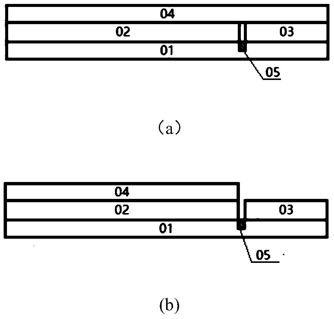
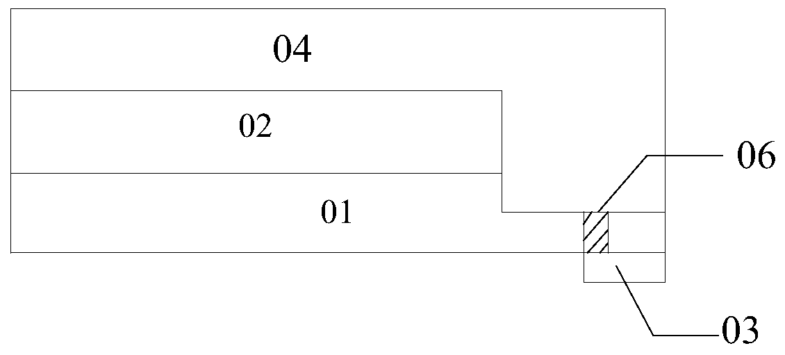
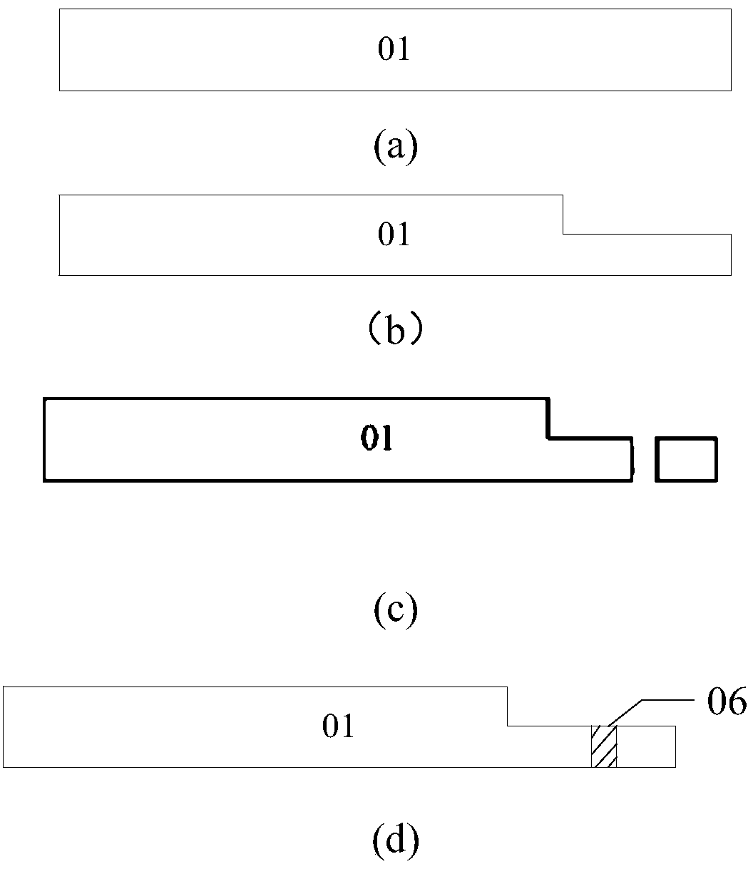
[0029] figure 2 The structure schematic diagram of the Micro OLED display structure provided by the embodiment of the present invention, for the convenience of description, only shows the part related to the embodiment of the present invention.
[0030] The structure includes:
[0031] Base, base comprises PAD connection area and non-PAD connection area, the base thickness of PAD connection area is thinner than the base thickness of non-PAD connection area, CMOS drive circuit is arranged on non-PAD connection area, forms CMOS driving substrate, is provided with in PAD connection area A number of TSV through-holes, metal posts mat...
PUM
| Property | Measurement | Unit |
|---|---|---|
| Thickness | aaaaa | aaaaa |
| Aperture | aaaaa | aaaaa |
| Thickness | aaaaa | aaaaa |
Abstract
Description
Claims
Application Information
 - R&D
- Intellectual Property
- Life Sciences
- Materials
- Tech Scout
- Unparalleled Data Quality
- Higher Quality Content
- 60% Fewer Hallucinations
Browse by: Latest US Patents, China's latest patents, Technical Efficacy Thesaurus, Application Domain, Technology Topic, Popular Technical Reports.
© 2025 PatSnap. All rights reserved.Legal|Privacy policy|Modern Slavery Act Transparency Statement|Sitemap|About US| Contact US: help@patsnap.com