Display device, display panel thereof, and OLED array substrate
A technology for array substrates and display areas, applied in identification devices, static indicators, instruments, etc., can solve problems such as inconsistency and out-of-synchronization of display screens, and achieve the effects of fewer connecting lines, reduced junctions, and better imaging effects
- Summary
- Abstract
- Description
- Claims
- Application Information
AI Technical Summary
Problems solved by technology
Method used
Image

Examples
Embodiment Construction
[0063] In order to make the above objects, features and advantages of the present invention more comprehensible, specific embodiments of the present invention will be described in detail below in conjunction with the accompanying drawings.
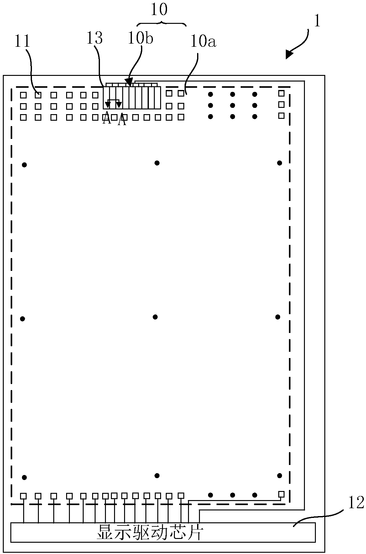
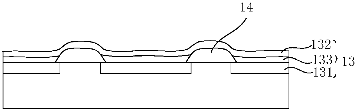
[0064] figure 1 is a top view of a display panel in an embodiment of the present invention; figure 2 is along figure 1 Sectional view of line AA in .
[0065] refer to figure 1 and figure 2 As shown, the display panel 1 includes: a display area 10, the display area 10 includes a non-transparent display area 10a and a transparent display area 10b;
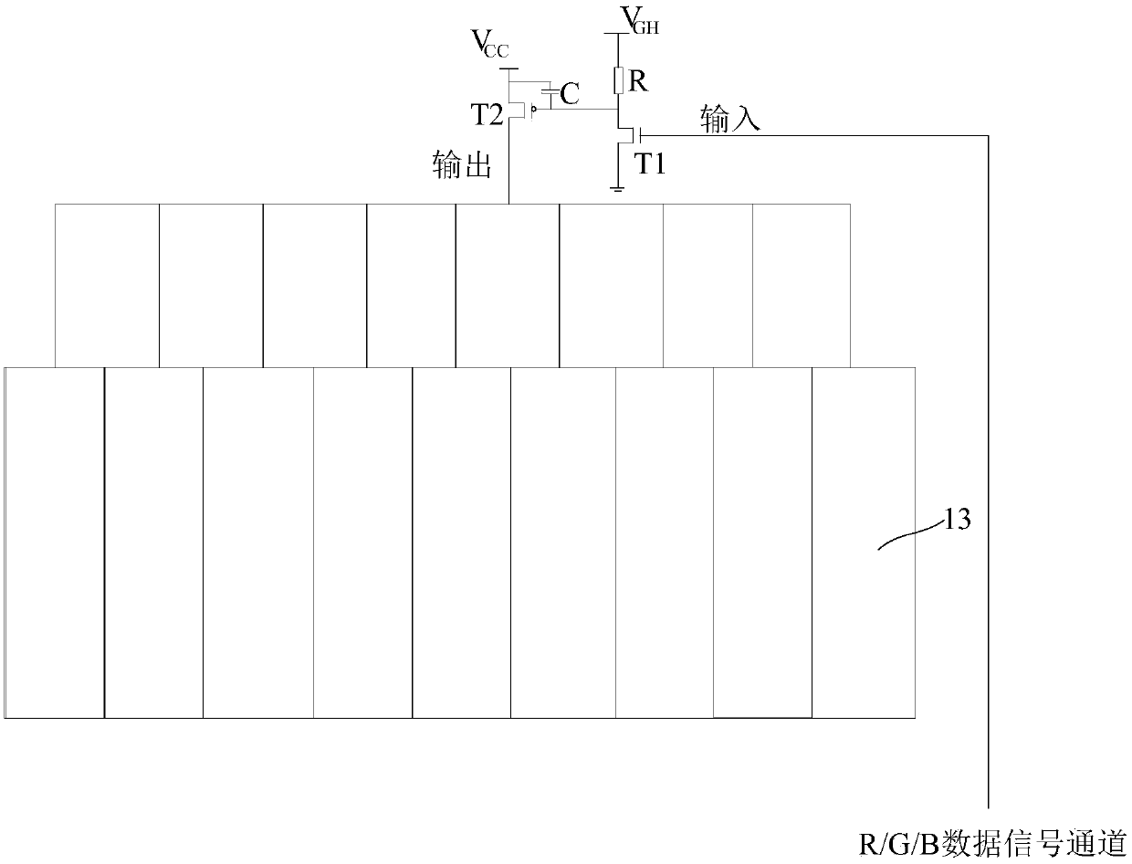
[0066] Among them, the non-transparent display area 10a includes first OLED pixels 11 arranged in an array, and the first OLED pixels 11 include from bottom to top: a block-shaped first electrode, an OLED light-emitting structure, and a second electrode; each column of first OLED pixels The driving mode of 11 is active, and the driving of each first OLED pixel 11 corresponds to the part n...
PUM
 Abstract
Description
Claims
Application Information
 - R&D
- Intellectual Property
- Life Sciences
- Materials
- Tech Scout
- Unparalleled Data Quality
- Higher Quality Content
- 60% Fewer Hallucinations
Browse by: Latest US Patents, China's latest patents, Technical Efficacy Thesaurus, Application Domain, Technology Topic, Popular Technical Reports.
© 2025 PatSnap. All rights reserved.Legal|Privacy policy|Modern Slavery Act Transparency Statement|Sitemap|About US| Contact US: help@patsnap.com