Method for fabricating semiconductor device and semiconductor device using the same

a semiconductor device and semiconductor technology, applied in semiconductor devices, transistors, decorative arts, etc., can solve the problems of time-consuming set-up and high cost of methods, and achieve the effects of reducing off-state leakage current, reducing junction capacitance, and improving pmos device characteristics

Active Publication Date: 2006-01-05
MARVELL ASIA PTE LTD +1
View PDF16 Cites 11 Cited by
  • Summary
  • Abstract
  • Description
  • Claims
  • Application Information

AI Technical Summary

Benefits of technology

[0007] An object of the present invention is to provide a method for fabricating a semiconductor device, which decreases an off-state leakage current of a PMOS transistor.
[0009] Another object of the present invention is to provide a method for fabricating a semiconductor device, which exhibits improved PMOS device characteristics, including is reduced off-state leakage current and junction capacitance, without transistor performance degradation or additional processing.
[0010] Another object of the present invention is to provide a method for fabricating a semiconductor device, which uses channel engineering to realize an improved PMOS device exhibiting reduced off-state leakage current and reduced junction capacitance.
[0011] Another object of the present invention is to provide a method for fabricating a semiconductor device, which increases chip speed.
[0012] Another object of the present invention is to provide a method for fabricating a semiconductor device, which enables pMOS device fabrication using a simple cost-effective technique.
[0016] According to the present invention, the implantation may be an implantation of 1.82×10¹³ atoms / cm2 performed at an energy level of 110 keV but is preferably a low-density implantation of 1.0×10¹²˜1.5×10¹³ atoms / cm2 performed at an energy level of 10˜100 keV, to reduce off-state leakage current and junction capacitance.

Problems solved by technology

Such methods, however, are costly and involve processes requiring time-consuming set-ups.

Method used


Image

  • Method for fabricating semiconductor device and semiconductor device using the same
  • Method for fabricating semiconductor device and semiconductor device using the same
  • Method for fabricating semiconductor device and semiconductor device using the same

Examples


Embodiment Construction

[0026] Reference will now be made in detail to the preferred embodiments of the present invention, examples of which are illustrated in the accompanying drawings. Wherever possible, like reference numbers will be used throughout the drawings to refer to the same or similar parts.

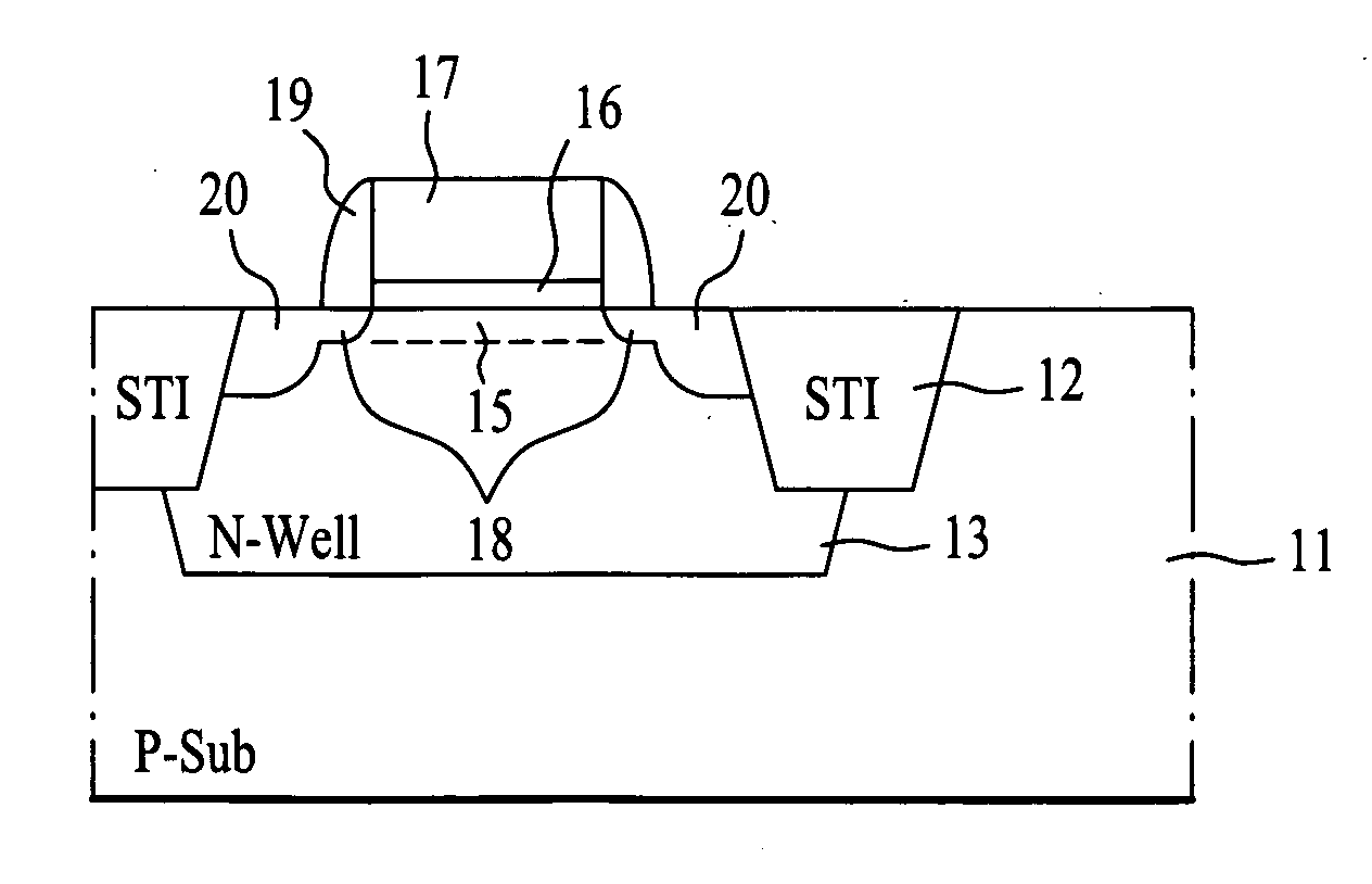
[0027] Low off-state leakage current (Ioff) can be obtained by increasing threshold voltage (Vth), but an increased threshold voltage results in higher gate edge junction leakage currents. Therefore, the present invention applies channel engineering to control the profile of a doped channel, namely, a channel ion implantation layer, to control the levels of gate edge junction leakage current. Also, the channel ion implantation process of the present invention can improve the chip's operating speed.

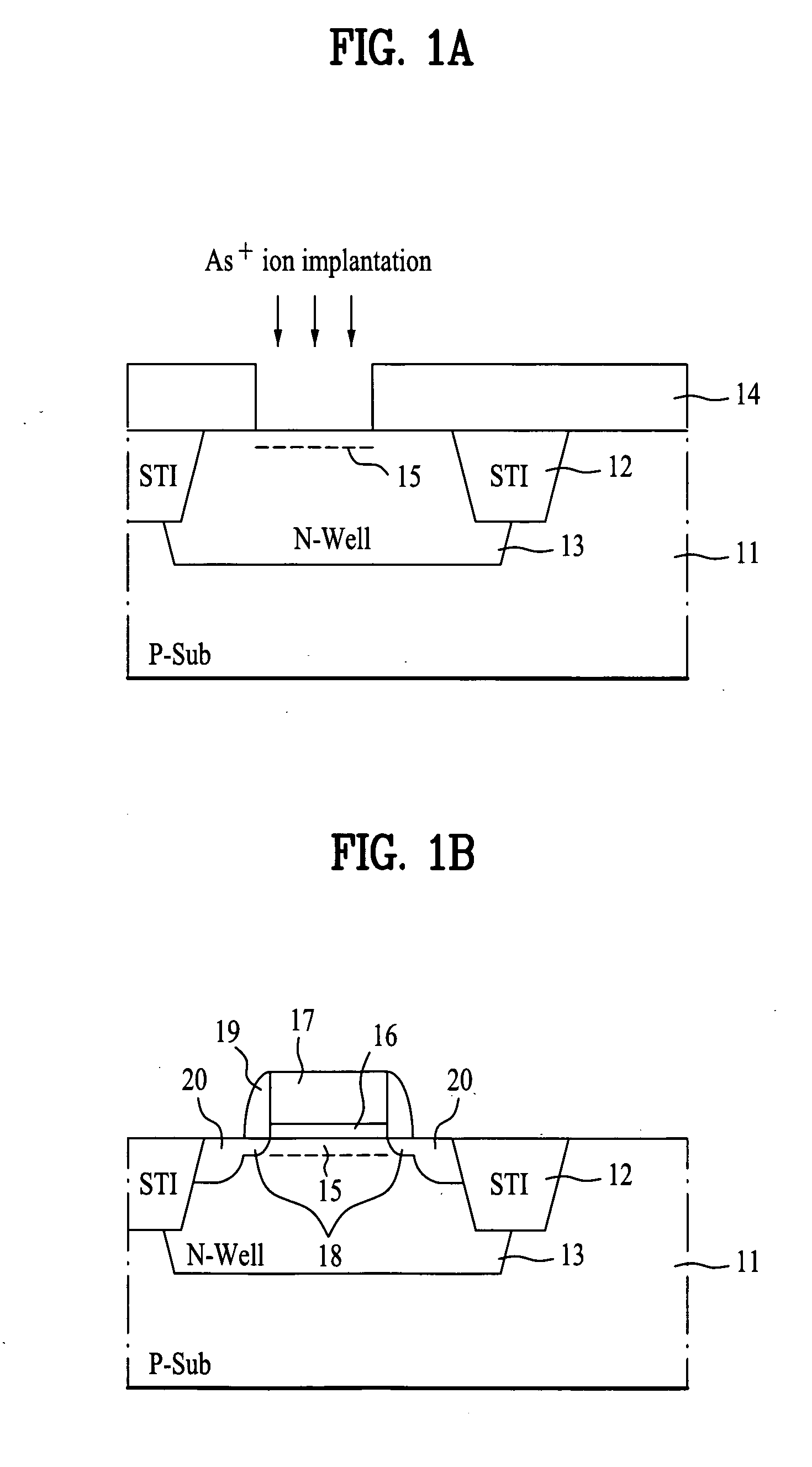
[0028] Referring to FIG. 1A, illustrating a pMOS transistor fabricated using 0.18 μm logic technology, an active area is defined by forming an N-well 13 in a p-type semiconductor substrate 11 having a shallow tre...


PUM

PropertyMeasurementUnit
energyaaaaaaaaaa
thicknessaaaaaaaaaa
gate lengthaaaaaaaaaa

Abstract

A method for fabricating a semiconductor device improves off-state leakage current and junction capacitance characteristics in a pMOS transistor. The method includes forming a device isolation layer defining an active area in a semiconductor substrate; and forming a channel ion implantation layer by an implantation of arsenic ions in a predetermined region of the active area of the semiconductor substrate at a predetermined density, the channel ion implantation layer having a predetermined doping profile according to the predetermined density of arsenic ion implantation. The implantation may be a low-density implantation of 1.0×10¹² ˜10×1013 atoms / cm2 performed at an energy level of 10˜100 keV.

Description

CROSS-REFERENCE TO RELATED APPLICATIONS [0001] This application claims the benefit of Korean Application No. 10-2004-0050360 filed on Jun. 30, 2004, which is hereby incorporated by reference as if fully set forth herein. BACKGROUND OF THE INVENTION [0002] 1. Field of the Invention [0003] The present invention relates to a semiconductor device, and more particularly, to a method for fabricating a semiconductor device, e.g., a positive-channel metal oxide semiconductor (PMOS) transistor device having improved leakage current (Ioff) and junction capacitance characteristics. [0004] 2. Discussion of the Related Art [0005] In fabricating a semiconductor device, for example, a pMOS device for use in portable electronics devices, there is a trade-off between high-performance and low off-state leakage current characteristics of the pMOS device. To achieve high-performance (e.g., high-speed) characteristics, the leakage current may be decreased by suppressing a gate-induced drain leakage curr...

Claims


Application Information

Patent Timeline
Patent Type & Authority Applications(United States)
IPC IPC(8): H01L21/04
CPCH01L21/26513H01L29/6659H01L29/105H01L21/18
Inventor BANG, KI WAN
Owner MARVELL ASIA PTE LTD
Why Eureka
Try Eureka