Nitride semiconductor light emitting device

a light-emitting device and nitride technology, applied in the field of semiconductor light-emitting devices, can solve the problems of poor reliability, gradual increase of leak current, poor yield, etc., and achieve the effects of enhancing yield, reliable, and nitride semiconductor light-emitting

Active Publication Date: 2012-12-04
SHARP FUKUYAMA LASER CO LTD
View PDF16 Cites 9 Cited by
  • Summary
  • Abstract
  • Description
  • Claims
  • Application Information

AI Technical Summary

Benefits of technology

[0013]The present invention is made to solve the aforementioned problems. An object of the present invention is to provide a reliable, nitride semiconductor light emitting device in which short-circuit at the PN junction portion and current leakage are reduced as compared with the conventional, and a method of manufacturing the same.
[0038]According to the present invention, the PN junction portion is coated with an insulating layer so that a source of leak current such as metal intrusion can be reduced, for example, in the step of forming the nitride semiconductor light emitting device wafer into chips, thereby enhancing the yield. In addition, it is possible to provide a reliable, nitride semiconductor light emitting device with less degradation even when the device is powered for a long time or fed with large current.

Problems solved by technology

In this case, a metal layer, for example, of gold (Au), indium, tin, solder, silver paste or the like, which is formed on the ohmic electrode to improve adhesiveness, extends off the chip end portion and extends behind, because of non-cleavability and high viscosity of these metals, to cause a short circuit at the PN junction portion, resulting in poor yields.
In addition, in the case where silver paste or the like is used as a metal layer, even when the initial property is normal, the leak current gradually increases after aging and the reliability is very poor as a light emitting device.
This increase of leak current may be attributable to leakage of metal from the metal layer.

Method used


Image

  • Nitride semiconductor light emitting device
  • Nitride semiconductor light emitting device
  • Nitride semiconductor light emitting device

Examples


first embodiment

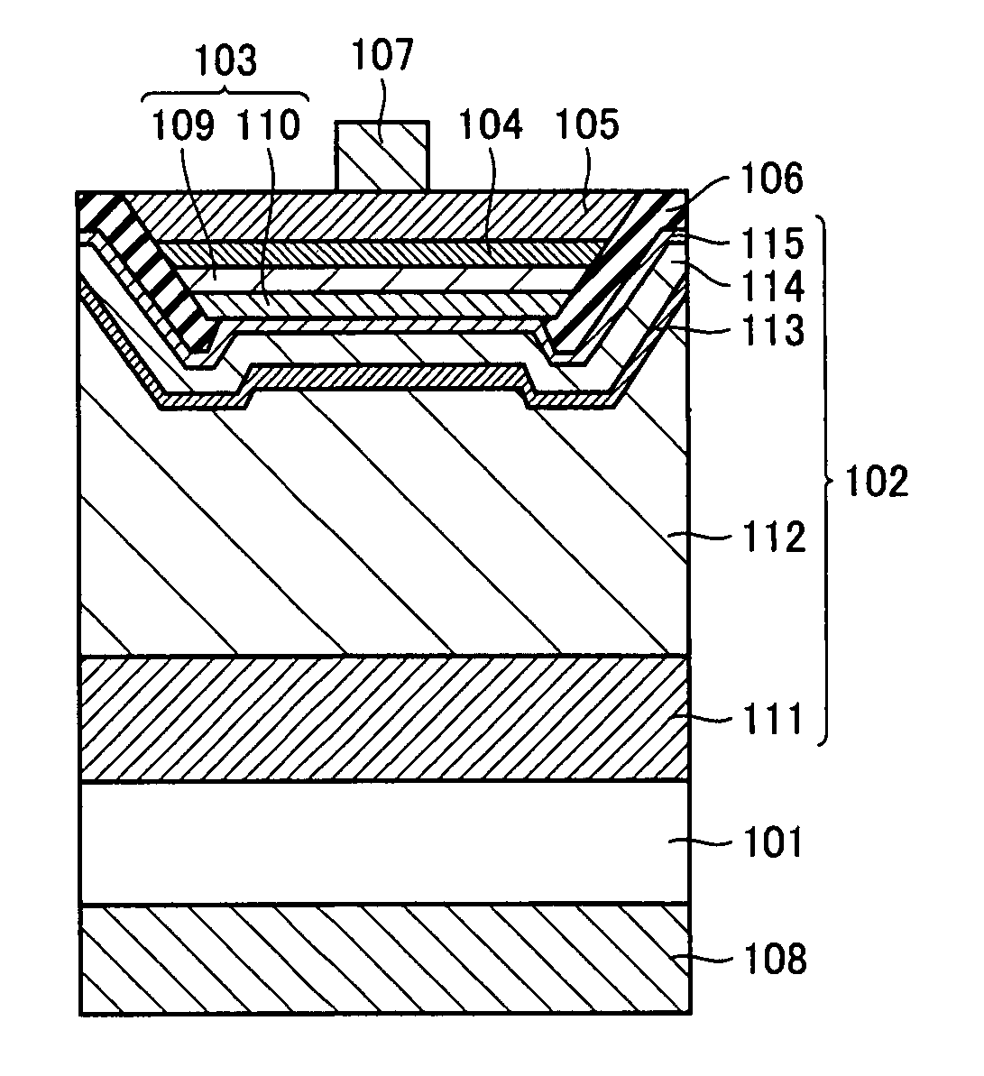
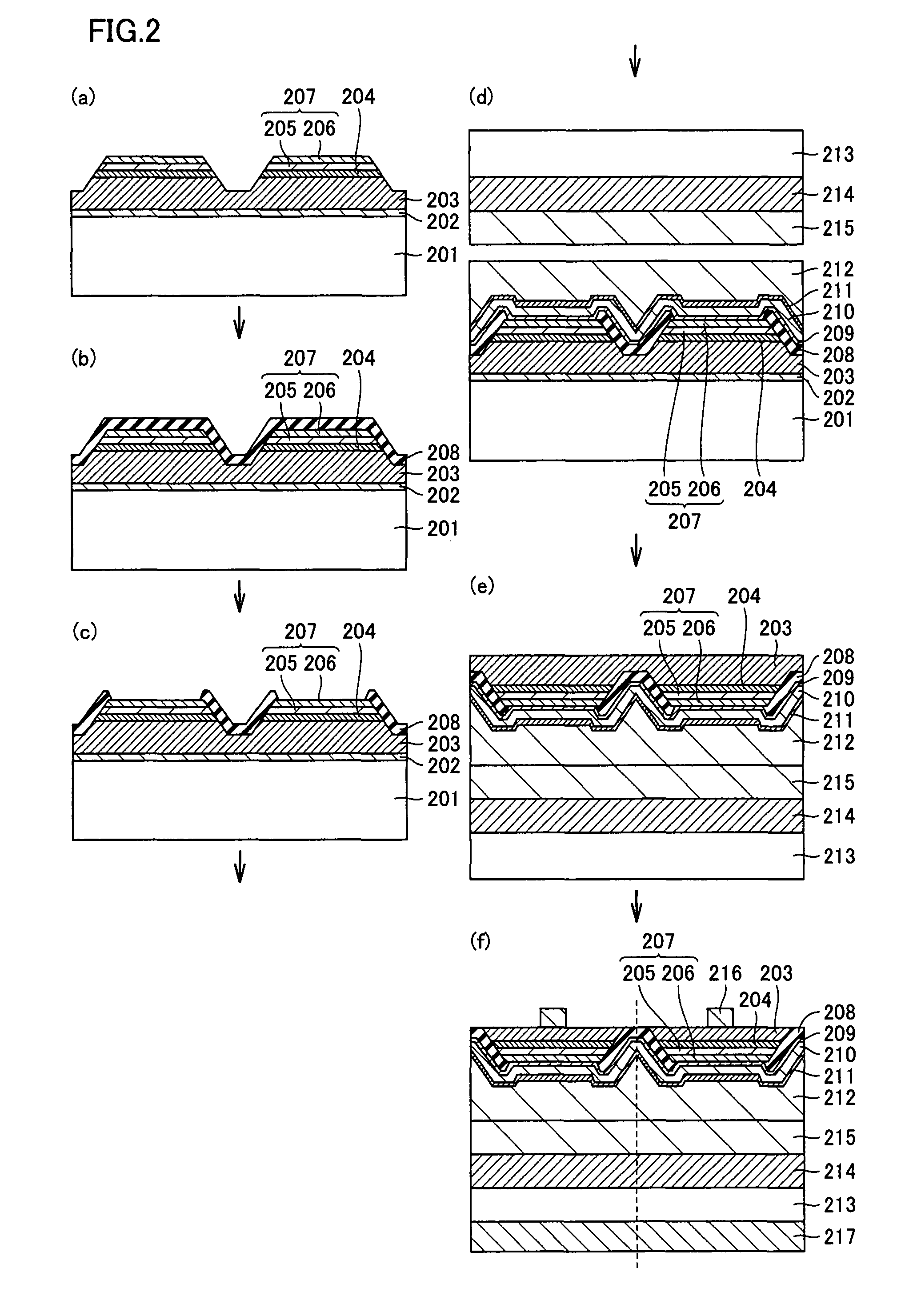
[0053]FIG. 1 is a schematic cross-sectional view showing a nitride semiconductor light emitting device in a preferable embodiment of the present invention. As shown in FIG. 1, the nitride semiconductor light emitting device in the present embodiment includes a conductive substrate 101, a first metal layer 102, a second conductivity-type semiconductor layer 103, an emission layer 104, and a first conductivity-type semiconductor layer 105, in this order. In addition, the nitride semiconductor light emitting device has an insulating layer 106 which covers the side surfaces of second conductivity-type semiconductor layer 103, emission layer 104 and first conductivity-type semiconductor layer 105 as well as part of that surface of second conductivity-type semiconductor layer 103 which is in contact with first metal layer 102. The nitride semiconductor light emitting device in the present embodiment additionally has a first electrode 107 for external connection formed on first conductivit...

second embodiment

[0117]FIG. 3 is a schematic cross-sectional view showing a nitride semiconductor light emitting device in another preferable embodiment of the present invention. As shown in FIG. 3, the nitride semiconductor light emitting device in the present embodiment includes a conductive substrate 301, a first metal layer 302, a second conductivity-type semiconductor layer 303, an emission layer 304, and a first conductivity-type semiconductor layer 305, in this order. In addition, the nitride semiconductor light emitting device in the present embodiment has an insulating layer 306, which covers the side surfaces of second conductivity-type semiconductor layer 303, emission layer 304 and first conductivity-type semiconductor layer 305 and, in addition, part of that surface of second conductivity-type semiconductor layer 303 which faces first metal layer 302. The nitride semiconductor light emitting device in the present embodiment has a first electrode 307 formed on first conductivity-type sem...

third embodiment

[0145]FIG. 5 is a schematic cross-sectional view showing a nitride semiconductor light emitting device in another preferable embodiment of the present invention. As shown in FIG. 5, the nitride semiconductor light emitting device in the present embodiment includes a conductive substrate 501, a first metal layer 502, a second metal layer 515, a second conductivity-type semiconductor layer 503, an emission layer 504, and a first conductivity-type semiconductor layer 505, in this order. In addition, the nitride semiconductor light emitting device in the present embodiment has an insulating layer 506, which covers the side surfaces of second metal layer 515, second conductivity-type semiconductor layer 503, emission layer 504 and first conductivity-type semiconductor layer 505 and part of that surface of second metal layer 515 which faces first metal layer 502. The nitride semiconductor light emitting device in the present embodiment has a first electrode 507 for external connection for...


PUM


Abstract

A nitride semiconductor light emitting device includes a conductive substrate, a first metal layer, a second conductivity-type semiconductor layer, an emission layer, and a first conductivity-type semiconductor layer in this order. The nitride semiconductor light emitting device additionally has an insulating layer covering at least side surfaces of the second conductivity-type semiconductor layer, the emission layer and the first conductivity-type semiconductor layer. A method of manufacturing the same is provided. The nitride semiconductor light emitting device may further include a second metal layer. Thus, a reliable nitride semiconductor light emitting device and a method of manufacturing the same are provided in which short-circuit at the PN junction portion and current leak is reduced as compared with the conventional examples.

Description

[0001]This nonprovisional application is based on Japanese Patent Applications Nos. 2006-220153 and 2007-143705 filed with the Japan Patent Office on Aug. 11, 2006 and May 30, 2007, respectively, the entire contents of which are hereby incorporated by reference.BACKGROUND OF THE INVENTION[0002]1. Field of the Invention[0003]The present invention relates to a semiconductor light emitting device using nitride semiconductor (InXAlYGa1-X-YN, 0≦X, 0≦Y, X+Y≦1) and a method of manufacturing the same.[0004]2. Description of the Background Art[0005]Nitride semiconductor receives attentions as a variety of semiconductor devices such as light emitting devices, and for example, blue LED (Light Emitting Diode), blue-green LED, and the like have been put to practical use.[0006]Conventionally, nitride semiconductor light emitting devices are manufactured by growing nitride semiconductor in a stacked manner on an insulative substrate such as sapphire, spinel, lithium niobate, or neodymium gallate. ...

Claims


Application Information

Patent Timeline
Patent Type & Authority Patents(United States)
IPC IPC(8): H01L33/00H01L33/06H01L33/10H01L33/14H01L33/22H01L33/32
CPCH01L33/0079H01L33/405H01L33/44H01L33/0093H01L21/027H01L21/28H01L21/78H01L33/0066H01L33/0075H01L33/486H01L33/62H01L2933/0033H01L2933/0066
Inventor FUDETA, MAYUKOTSUNODA, ATSUO
Owner SHARP FUKUYAMA LASER CO LTD
Why Eureka
Try Eureka