Multi-wavelength InGaN/GaN multi-quantum well structure based on GaN dodecahedral cone and preparation method thereof

A multi-quantum well structure and multi-quantum well layer technology, which is applied in the field of semiconductor light-emitting devices, can solve the problems of reducing the working efficiency and device life of semiconductor components, affecting the performance stability of GaN-based optoelectronic devices, surface damage and pollution, and achieving realization Large-scale growth and application, improved internal quantum efficiency, and low cost effects

Inactive Publication Date: 2020-02-07
张士英
View PDF4 Cites 2 Cited by
  • Summary
  • Abstract
  • Description
  • Claims
  • Application Information

AI Technical Summary

Problems solved by technology

These dislocations act as non-radiative centers, causing the incoming energy to dissipate in the form of heat. Heat has a great impact on semiconductors and will reduce the working efficiency and device life of semiconductor components.
In addition, the stress distribution in the cone axis is not uniform, re

Method used


Image

  • Multi-wavelength InGaN/GaN multi-quantum well structure based on GaN dodecahedral cone and preparation method thereof
  • Multi-wavelength InGaN/GaN multi-quantum well structure based on GaN dodecahedral cone and preparation method thereof
  • Multi-wavelength InGaN/GaN multi-quantum well structure based on GaN dodecahedral cone and preparation method thereof

Examples


Embodiment Construction

[0035] The present invention will be further elaborated below in conjunction with the accompanying drawings and specific embodiments.

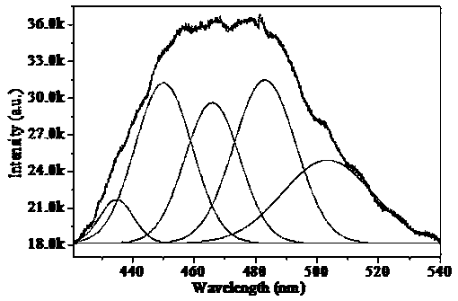
[0036] A multi-wavelength InGaN / GaN multiple quantum well structure based on GaN dodecahedral cones, through thermal H 4 PO 3 Etch the N-face self-supporting GaN substrate material to form a micro-nano GaN dodecahedron structure; use H 4 PO 3 The solution is heated and etched, and the micro-nano GaN dodecahedron is obtained by etching, and the InGaN / GaN multiple quantum well layer is grown on the GaN dodecahedron template by using metal organic chemical vapor phase epitaxy (MOCVD).

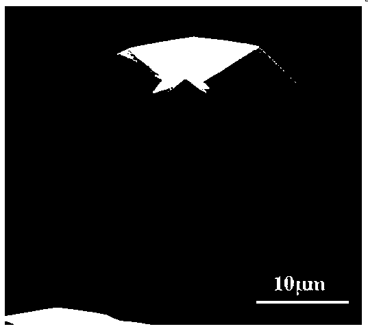
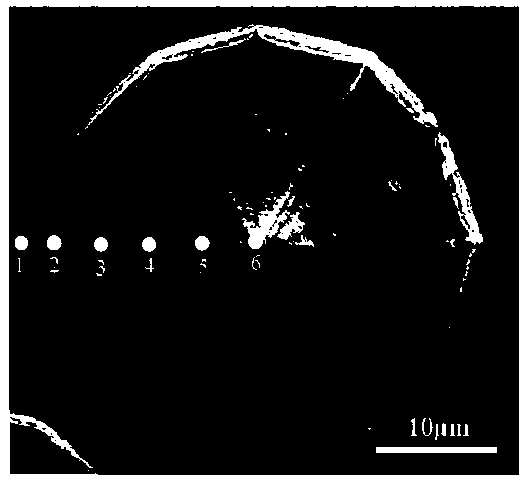
[0037] Such as figure 1 As shown, the micro-nano GaN dodecahedron is a dodecahedron composed of twelve triangular faces, and the space group of the wurtzite structure is , there are hexagonal rotational symmetry and mirror symmetry. The twelve-sided cone reflects the symmetry of the wurtzite structure. The structure of the twelve-sided cone is composed of six...


PUM

PropertyMeasurementUnit
Thicknessaaaaaaaaaa
Thicknessaaaaaaaaaa

Abstract

The invention discloses a multi-wavelength InGaN/GaN multi-quantum well structure based on a GaN dodecahedral cone and a preparation method thereof. An N-surface self-supporting GaN substrate materialis corroded through hot H4PO3 to form a micro-nano GaN dodecahedral cone structure; stress in the GaN dodecahedral cone obtained through corrosion is greatly released, so that the crystal quality ofa sample can be effectively improved, the luminous efficiency can be effectively improved, and subsequent epitaxial regrowth is facilitated; and an InGaN/GaN multi-quantum well layer is grown on a GaNdodecahedral cone template by using the metal organic chemical vapor phase epitaxy technology. According to the method, different sizes of cones can be obtained by controlling the concentration of the corrosive liquid, the corrosion temperature and the corrosion time; white light emitting can be achieved by reasonably adjusting the size of the cone and the In component; and the method is a possible way for achieving single-chip fluorescent-powder-free white light emitting. The method provided by the invention does not need a patterned substrate, is low in process cost, is simple and feasible,and is suitable for large-scale preparation.

Description

technical field [0001] The invention relates to the field of semiconductor light-emitting devices, in particular to a GaN dodecahedron-based multi-wavelength InGaN / GaN multi-quantum well structure and a preparation method thereof. Background technique [0002] Among wide-bandgap and direct-gap semiconductors, GaN-based semiconductors have the most development potential and development prospects. With their wide bandgap [0.64 eV (InN), 3.4eV (GaN), 6.2eV, (AlN)] and superior The performance (thermal stability, chemical stability and high thermal conductivity, etc.) has become a hot spot and focus in the research of optoelectronic materials and devices in recent years. On the other hand, InGaN light-emitting diodes (LEDs) can cover the entire visible wavelength range, thus attracting great attention in applications such as color displays and general lighting equipment. However, these InGaN / GaN materials still have inherent difficulties that need to be overcome before the ulti...

Claims


Application Information

Patent Timeline
IPC IPC(8): H01L33/06H01L33/16H01L33/20H01L33/32H01L33/00
CPCH01L33/0075H01L33/06H01L33/16H01L33/20H01L33/32
Inventor 张士英徐庆君许亮修向前赵红华雪梅谢自力韦德泉李振华
Owner 张士英
Why Eureka
Try Eureka