Chip testing device and system

A technology of chip testing and testing equipment, which is applied in the direction of measuring equipment, non-contact testing, single semiconductor device testing, etc., can solve the problems of inability to obtain hotspot positioning points, inability to use laser hotspot mode, etc., to improve the test range and expand the test function, cost reduction effect

Pending Publication Date: 2020-02-11
YANGTZE MEMORY TECH CO LTD
View PDF0 Cites 3 Cited by
  • Summary
  • Abstract
  • Description
  • Claims
  • Application Information

AI Technical Summary

Problems solved by technology

However, when the test machine is used to apply signals to the chip, since the test machine cannot be connected to an external power source, the laser hotspot mode cannot be used to locate the laser hot spot, so a more accurate hot spot location cannot be obtained.

Method used


Image

  • Chip testing device and system
  • Chip testing device and system
  • Chip testing device and system

Examples


Embodiment Construction

[0028] Various embodiments of the invention will be described in more detail below with reference to the accompanying drawings. In the various drawings, the same elements are denoted by the same or similar reference numerals. For the sake of clarity, various parts in the drawings have not been drawn to scale.

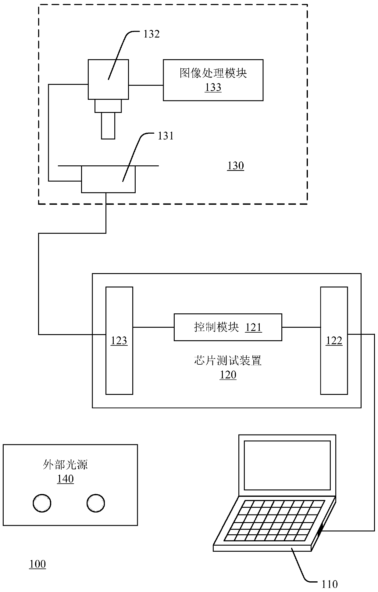
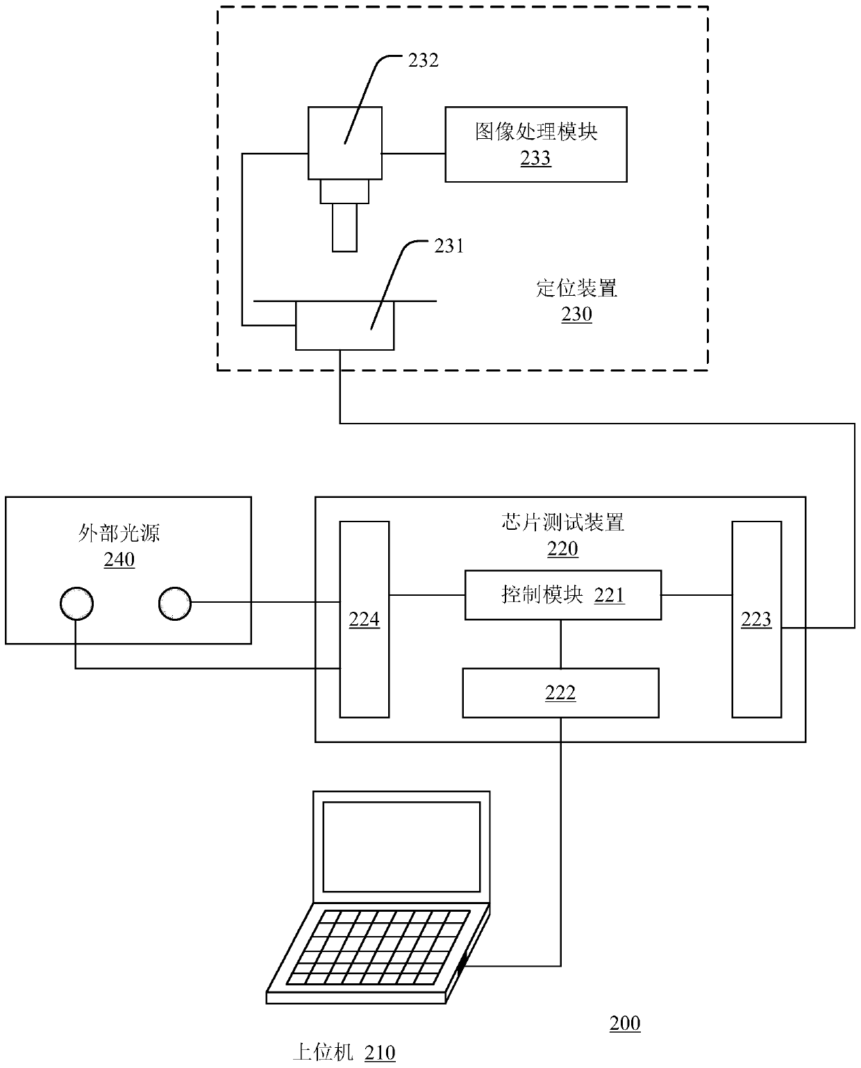
[0029] figure 1 A prior art chip testing system 100 is shown. The chip testing system 100 includes a host computer 110 , a testing device 120 and a positioning device 130 .

[0030] Wherein, the upper computer 110 is, for example, a server that can control all operations in chip testing, and is used to generate control signals, and the control signals are, for example, used to control logic management and processes in the chip testing process. Among them, logic management includes the working state or test mode of the chip during testing. This working state is a certain state, such as Program (writing), Erase (erasing) or Read (reading). In this state, , the chip to...


PUM


Abstract

The application discloses a chip testing device and system. The chip testing device comprises an upper computer interface connected with an upper computer and used for receiving a control signal fromthe upper computer so as to control a testing mode of the chip; a testing interface connected with a chip and used for providing a testing signal corresponding to the testing mode for the chip; a light source interface connected with an external light source and used for providing a light source signal for the external light source; and a control module connected with the upper computer interface,the testing interface and the light source interface, wherein the control module controls the light source signal according to the testing signal, so that the external light source and a testing timesequence of the chip are synchronously started and closed. The light source interface is added on the testing device disclosed by the application, and the testing function of the chip testing deviceis expanded through the connection of the light source interface and the external light source.

Description

technical field [0001] The invention relates to the technical field of semiconductor testing and analysis, in particular to a chip testing device and system. Background technique [0002] With the rapid development of semiconductor device and circuit manufacturing technology, the feature size of the device is continuously reduced, while the integration level is continuously increased. Changes in these two aspects bring great challenges to failure defect location and failure mechanism analysis. EMMI (Emission Microscope) technology, as a new type of high-resolution microscopic defect localization technology, can quickly and accurately locate device failures in a wide range, so it is widely used in device failure analysis. Optical Emission Microscope (EMMI) and Optical Beam Induced Resistance Change (OBIRCH, Optical Beam Induced Resistance Change) functions are often integrated in one detection system to synthesize PEM (Photo Emission Microscope). The two complement each othe...

Claims


Application Information

Patent Timeline
Patent Type & Authority Applications(China)
IPC IPC(8): G01R31/265G01R31/26
CPCG01R31/2601G01R31/2656
Inventor 官绪冬吴继君
Owner YANGTZE MEMORY TECH CO LTD
Why Eureka
Try Eureka