Dielectric film and its preparation method
A technology of dielectric film and dielectric constant, applied in circuits, capacitors, electrical components, etc., can solve problems such as limited space for improvement, doping, etc., and achieve the effects of improving energy storage characteristics, increasing breakdown electric field, and improving leakage performance
- Summary
- Abstract
- Description
- Claims
- Application Information
AI Technical Summary
Problems solved by technology
Method used
Image
Examples
preparation example Construction
[0026] The preparation method of a double dielectric energy transfer film includes the following steps:
[0027] Step 1: Use the interface charge accumulation model to pre-screening materials, using the following formula
[0028]
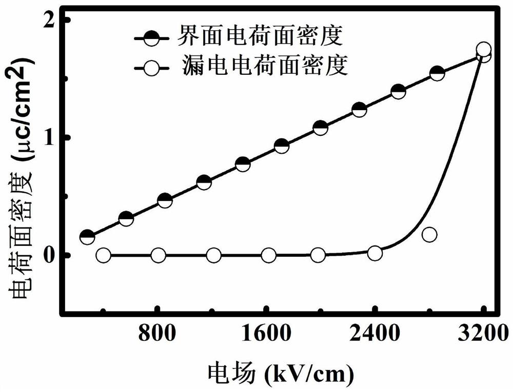
[0029] Among them, ε 0 Ε 1 Ε 2 It is a vacuum dielectric constant, the dielectric constant of the raw material 1 and the dielectric constant of the raw material 2, D. 1 And D 2 The thickness of the raw material 1 and the thickness of the raw material 2, respectively, γ 1 And gamma 2 The conductivity of the raw material 1 and the electrical conductivity of the raw material 2, respectively, U respects the voltage applied to the double layer dielectric material. By this formula, the leakage charge surface density σi capable of accommodating at the interface can be calculated and the specific value is obtained.
[0030] Step 2: Selecting the energy storage performance relatively good, but the dielectric constant and the conductivity differ, which are mate...
Embodiment 1
[0038] Implement example 1NA 0.5 BI 3.25 La 1.25 Ti 4 O 15 / BABI 3.4 La 0.6 Ti 4 O 15 Double-layer dielectric index film
[0039] Using the following raw materials (whose purity is analyzed, the purity is 99.9% or more), and the interface charge accumulation model is used; NA is prepared using a hierarch and fast annealing furnace. 0.5 BI 3.25 La 1.25 Ti 4 O 15 / BABI 3.4 La 0.6 Ti 4 O 15 Double dielectric energy transfer film.
[0040] The following is a double-layer dielectric energy film Na for preparing high storage performance. 0.5 BI 3.25 La 1.25 Ti 4 O 15 / BABI 3.4 La 0.6 Ti 4 O 15 The specific steps.
[0041] 1.1): Adopt the interface charge accumulation model to bring the dielectric constant and conductivity of the original material, obtain the thickness ratio 19: 16 of the two materials, and obtain the leakage charge surface density capable of receiving the interface.
[0042] 1.2): 0.6496 g of six hydrazine nitrate, 4.5812 g of five hydrated nitrate, 0.645 g of hydroc...
Embodiment 2
[0049] Example 2NA 0.5 BI 3 La 1.5 Ti 4 O 15 / BABI 3.1 La 0.9 Ti 4 O 15 Double-layer dielectric index film
[0050] Using the following raw materials (whose purity is analyzed, the purity is 99.9% or more), and the interface charge accumulation model is used; NA is prepared using a hierarch and fast annealing furnace. 0.5 BI 3 La 1.5 Ti 4 O 15 / BABI 3.1 La 0.9 Ti 4 O 15 Double dielectric energy transfer film.
[0051] The following is a double-layer dielectric energy film Na for preparing high storage performance. 0.5 BI 3 La 1.5 Ti 4 O 15 / BABI 3.1 La 0.9 Ti 4 O 15 The specific steps.
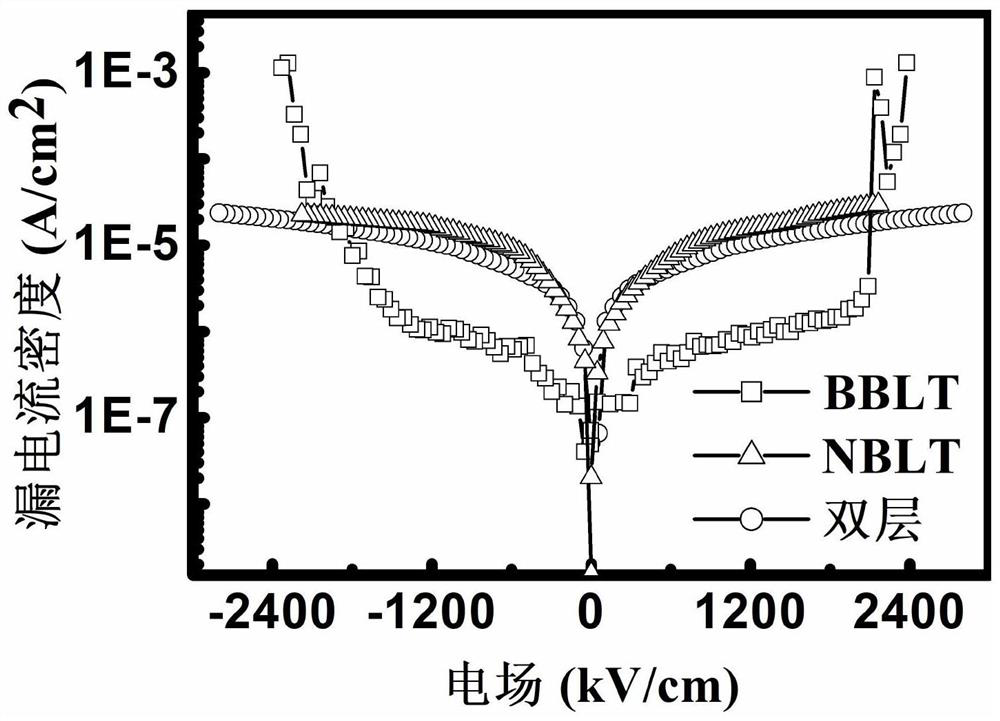
[0052] 1.1): Adopt interface charge accumulation model, where NA 0.5 BI 3 La 1.5 Ti 4 O 15 Babi 3.1 La 0.9 Ti 4 O 15 The dielectric constant is 352 and 408, respectively, and the conductivity obtains the conductivity of different electric fields according to the formula γ = j / e, and the leakage test results are obtained from the electrical conductivity of different electric fields, and the th...
PUM
 Abstract
Description
Claims
Application Information


