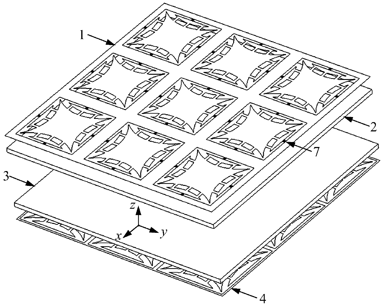
[0026] A device capable of realizing strong electromagnetic field protection in an ultra-wide frequency band, comprising an active frequency selective surface 1, an upper dielectric substrate 2, a lower dielectric substrate 3, and a bandpass frequency selective surface 4;
[0027] The active frequency selective surface 1 is printed on the upper surface of the upper dielectric substrate 2; the bandpass frequency selective surface 4 is printed on the lower surface of the lower dielectric substrate 3; the space between the upper dielectric substrate 2 and the lower dielectric substrate 3 is air layer; the axis of the active frequency selective surface 1, the axis of the upper dielectric substrate 2, the axis of the lower dielectric substrate 3, and the axis of the bandpass frequency selective surface 4 coincide;
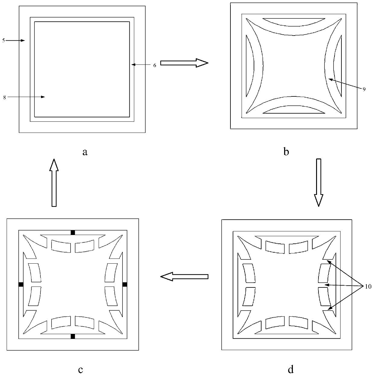
[0028] The active frequency selection surface 1 is composed of M×M units, each unit is a square metal patch 5 , and a square annular slot 6 is etched on the square metal patch 5 . A PIN diode 7 is connected across the gap; an arc-shaped slot 9 with a radius of R is etched on the inner patch 8 surrounded by the square annular slot 6, and three equidistant arrays are loaded on the arc-shaped slot 9 The rectangular patch 10;
[0029] The bandpass frequency selection surface 4 is composed of M×M units, each unit is a square metal patch 11 , and a square annular slot 12 is etched on the square metal patch 11 ; A circular arc-shaped slit 14 with a radius S is etched on the enclosed inner patch 13, and three rectangular patches 15 arranged at equal intervals are loaded on the circular arc-shaped slit 14;
[0030] In specific implementation, M=20, R=8.15mm, and S=9.4mm.
[0031] like Figure 4 As shown, the curve I represents the transmission coefficient S of the active frequency selective surface under the condition of low power signal incidence 21 , curve II represents the transmission coefficient S of the guard under the condition of low-power signal incidence 21. pass Figure 4 It can be seen that the active frequency selective surface resonates at 3.46GHz with an insertion loss of 0.33dB. Working bandwidth (|S 11 |< -10 dB) for 3.3-3.65GHz. In addition, the active frequency selective surface also resonates at 10.37 GHz and 15.56 GHz. After the introduction of the band-pass frequency selective surface, since the electromagnetic protection device becomes a double-layer structure, the operating frequency band is broadened (3.28GHz-3.92GHz), the relative bandwidth reaches 17.78%, and the insertion loss increases to 0.72dB.
[0032] like Figure 5 As shown, the curve I represents the transmission coefficient S of the active frequency selective surface under the condition of high power signal incidence21 , curve II represents the transmission coefficient S of the guard under the condition of high-power signal incidence 21. pass Figure 5 It can be seen that when a high-power signal is incident, the induced voltage is greater than the threshold voltage, the diode is turned on, the resonance point of the active frequency selective surface is shifted to the right, and the shielding efficiency in the passband increases to 17dB, but the active frequency selective surface is 7.76GHz. The HPM loses its protective effect. After adding the ideal bandpass frequency selection surface, the transmission loss at 7.76GHz increases by 12.5dB, and finally, the shielding effectiveness of the protective device is always greater than 13dB in the ultra-wideband range of 0-20GHz.
[0033] like Image 6 As shown, curve I represents the transient response when the active frequency selective surface is excited by a modulated sine plane wave with an electric field strength of 10 V/m, and curve II represents the transient response when the protective device is excited by a modulated sine plane wave with an electric field strength of 10 V/m. pass Image 6 It can be seen that both the active frequency selective surface and the protective device work in the transmission state, and the waveform of the transmitted signal is basically the same as that of the incident signal. Among them, the maximum field strength of the transmission signal of the active frequency selection surface is 8.4V/m, and the maximum field strength of the transmission signal of the protective device is 8.3V/m. The insertion loss is about 0.1dB higher than that of the active frequency selection surface. The effect of transmission is basically negligible.
[0034] like Figure 7 As shown, curve I represents the transient response when the active frequency selective surface is excited by a modulated sine plane wave with an electric field strength of 2000 V/m, and curve II represents the transient response when the protective device is excited by a modulated sine plane wave with an electric field strength of 2000 V/m. pass Image 6 It can be seen that both the active frequency selection surface and the protective device work in the protective state, and the transmitted signal waveform is obviously distorted compared with the incident signal. The maximum field strength of the transmission signal of the active frequency selection surface is 797V/m, and the maximum field strength of the transmission signal of the protective device is 315V/m. The invention obviously reduces the peak leakage and improves the protection ability to HPM.
[0035] Figure 8 It is a schematic diagram of the transmission field strength of the present invention under different incident field strength conditions. Depend on Figure 8 It can be seen that when the incident field strength gradually increases from 0V/m to 80V/m, the transmitted field strength increases linearly with the incident field strength. As the field strength continues to increase, the diode starts to conduct gradually, and the transmitted field strength exhibits a nonlinear change with the incident field strength.
[0036] Figure 9 It is a schematic diagram showing the variation of the shielding effectiveness with the incident wave field intensity of the present invention. Depend on Figure 9 It can be seen that the shielding effectiveness SE varies with the incident field strength in the range of 2-20 dB. When the electric field strength varies in the range of 0-80V/m, the protective device is in a stable transmission state, and the in-band insertion loss is 2dB. As the field strength gradually increases, the diode on the protective device is partially turned on, and the shielding effectiveness SE The field strength E increases linearly. When the field strength increases to 600V/m, the diodes are all turned on, the protective device is in a stable protection state, and the shielding effectiveness SE is stable above 17dB, but there are obvious fluctuations with the increase of the field strength. exist Figure 9 It can be seen that there are two obvious inflection points, one is the incident field strength E=80V/m, at this time the diode has just started to conduct. The second is the incident field strength E=600V/m, at this time the diodes are all turned on.